|
The Output Types | Max. Wire | Wire Gauge | |
of the Encoder | Length | ||
|
Wiring Diagram 1
Jumper
Braking Resistor(Option)
Voltage | 50m | |
|
| 1.25mm2(AWG18) or above |
|
| |
Open Collector | 50m | |
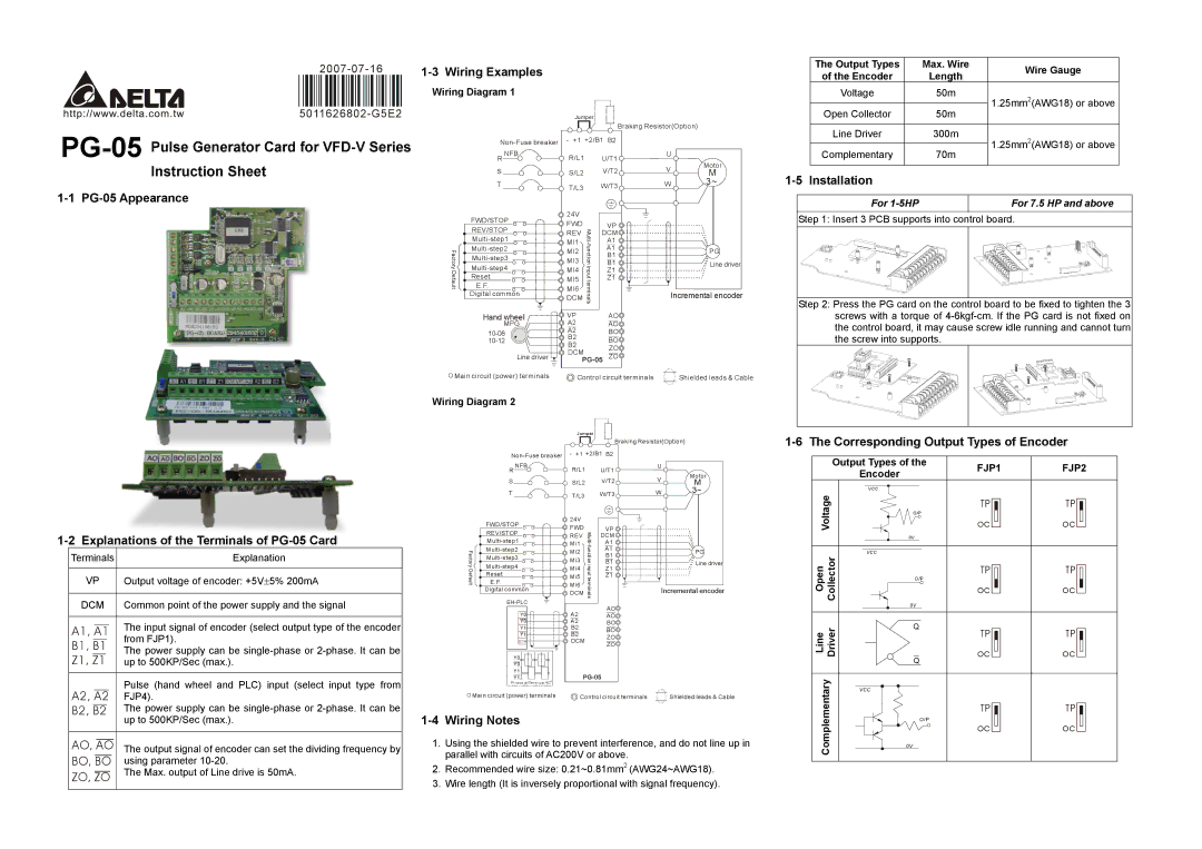
1-1 PG-05 Appearance
Factory Default![]()
![]()
- +1 +2/B1 B2 | ||||
R NFB | R/L1 |
| U/T1 | |
S | S/L2 |
| V/T2 | |
T | T/L3 |
| W/T3 | |
FWD/STOP | 24V |
|
| |
FWD |
| VP | ||
REV/STOP | Multi- | |||
REV | DCM | |||
MI1 | A1 | |||
MI3 | function | B1 | ||
MI2 |
| B1 | ||
|
| |||
|
|
| ||
MI4 | input | Z1 | ||
Reset | MI5 | Z1 | ||
E.F. | MI6 | terminals |
| |
|
| |||
Digital common |
|
| ||
DCM |
|
| ||
|
|
| ||
Hand wheel | VP |
| AO | |
MPG | A2 |
| AO | |
A2 |
| BO | ||
B2 |
| BO | ||
B2 |
| |||
|
| ZO | ||
| DCM |
| ||
Line driver |
| ZO | ||
|
| |||
U |
| |
V | Motor | |
M | ||
|
W3~
![]() PG
PG
![]()
![]()
![]() Line driver
Line driver
Incremental encoder
Line Driver | 300m | |
|
| 1.25mm2(AWG18) or above |
Complementary |
| |
70m | ||
1-5 Installation
For | For 7.5 HP and above |
Step 1: Insert 3 PCB supports into control board.
Step 2: Press the PG card on the control board to be fixed to tighten the 3 screws with a torque of
Main circuit (power) terminals | Control circuit terminals | Shielded leads & Cable |
Wiring Diagram 2
Jumper
Braking Resistor(Option)
Terminals | Explanation | |
|
| |
VP | Output voltage of encoder: +5V±5% 200mA | |
|
| |
DCM | Common point of the power supply and the signal | |
|
| |
A1, | The input signal of encoder (select output type of the encoder | |
B1, B1 | from FJP1). | |
The power supply can be | ||
Z1, Z1 | ||
up to 500KP/Sec (max.). | ||
|
| |
| Pulse (hand wheel and PLC) input (select input type from |
Factory Default![]()
![]()
- +1 +2/B1 B2 | ||||
R NFB | R/L1 |
| U/T1 | |
S | S/L2 |
| V/T2 | |
T | T/L3 |
| W/T3 | |
FWD/STOP | 24V |
|
| |
FWD |
| VP | ||
REV/STOP | Multi- | |||
REV | DCM | |||
Mi1 | A1 | |||
Mi3 | function | B1 | ||
Mi2 |
| B1 | ||
|
| |||
|
|
| ||
Mi4 | input | Z1 | ||
Reset | Mi5 | Z1 | ||
E.F. | Mi6 | terminals |
| |
|
| |||
Digital common |
|
| ||
DCM |
|
| ||
|
|
| ||
|
| AO | ||
Y0 | A2 |
| ||
| AO | |||
Y0 | A2 |
| BO | |
Y1 | B2 |
| BO | |
Y1 | B2 |
| ||
| ZO | |||
COM | DCM |
| ||
| ZO | |||
|
|
| ||
Y0 |
|
|
| |
Y0 |
|
|
| |
Y1 |
|
|
| |
Y1 |
|
|
| |
Phase difference 90o |
|
|
| |
U |
| |
V | Motor | |
M | ||
|
W3~
![]()
![]() PG
PG
![]()
![]()
![]() Line driver
Line driver
Incremental encoder
Output Types of the | FJP1 | FJP2 | |
| Encoder | ||
|
|
| |
Voltage | VCC |
|
|
| TP | TP | |
O/P |
|
| |
| oc | oc | |
|
|
| |
| 0V |
|
|
Open Collector | VCC |
|
|
| TP | TP | |
O/P |
|
| |
| oc | oc | |
|
|
| |
| 0V |
|
|
Line Driver | Q | TP | TP |
| |||
Q | oc | oc | |
|
|
| |
A2, A2 | FJP4). |
B2, B2 | The power supply can be |
| up to 500KP/Sec (max.). |
|
|
AO, AO | The output signal of encoder can set the dividing frequency by |
BO, BO | using parameter |
ZO, ZO | The Max. output of Line drive is 50mA. |
|
Main circuit (power) terminals | Control circuit terminals | Shielded leads & Cable |
1-4 Wiring Notes
1.Using the shielded wire to prevent interference, and do not line up in parallel with circuits of AC200V or above.
2.Recommended wire size: 0.21~0.81mm2 (AWG24~AWG18).
3.Wire length (It is inversely proportional with signal frequency).
Complementary | VCC |
|
TP | TP | |
O/P |
| |
oc | oc | |
0V |
| |
|
|