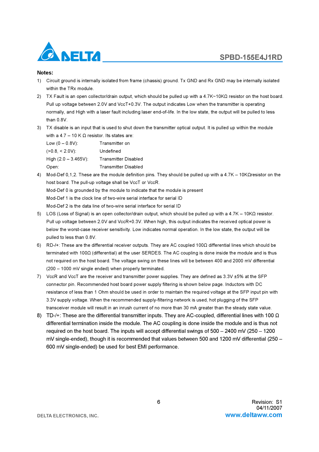
SPBD-155E4J1RD specifications
Delta Electronics has long been recognized as a leader in the design and manufacturing of high-quality power supplies and industrial automation equipment. One of their standout products is the SPBD-155E4J1RD, a sophisticated power supply designed for various industrial applications. This unit exemplifies Delta's commitment to innovation, efficiency, and reliability.The SPBD-155E4J1RD features a compact and lightweight design, a significant advantage for high-density installations. Weighing in at a modest 1.4 kg, it is engineered to fit seamlessly into tight spaces without sacrificing performance. A key aspect of its design is the ability to deliver stable and efficient power output, providing users with confidence in its performance during demanding operations.
Equipped with advanced Power Factor Correction (PFC) technology, the SPBD-155E4J1RD minimizes energy losses and maximizes efficiency. With a power rating of 155W and an input voltage range of 90-264 VAC, this unit ensures compatibility with various power systems across the globe. This feature not only enhances energy efficiency but also complies with international standards for energy conservation, helping users reduce their carbon footprint.
The SPBD-155E4J1RD utilizes a sophisticated cooling system that leverages a built-in fan, ensuring optimal performance by maintaining safe operating temperatures even during prolonged use. Furthermore, it boasts primary and secondary overload, overvoltage, and short-circuit protection features that safeguard connected devices, thus enhancing system reliability and longevity.
Designed for easy integration and operation, the SPBD-155E4J1RD includes user-friendly indicators for output status and alarms. This functionality allows operators to monitor the power supply's performance in real-time, facilitating quick troubleshooting and minimizing downtime.
The construction quality of the SPBD-155E4J1RD is another distinguishing feature, as it adheres to rigorous standards for electromagnetic compatibility and safety. It meets UL, CE, and other global certifications, ensuring that it operates safely and complies with industry regulations.
Overall, the Delta Electronics SPBD-155E4J1RD stands out in the market due to its blend of compact design, high efficiency, advanced safety features, and robust protection mechanisms. Whether used in industrial automation, telecommunications, or other demanding applications, this power supply remains a reliable choice for professionals seeking performance and durability.

