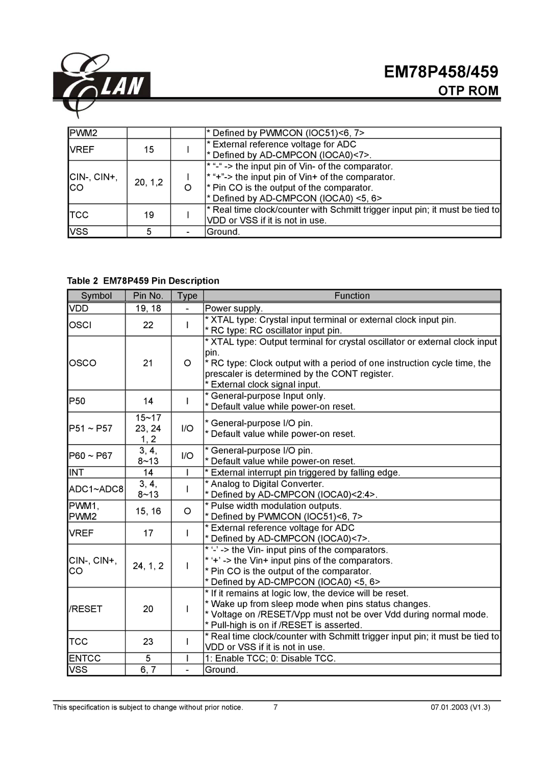
EM78P458, EM78P459AM, EM78P458AM, EM78P459AK, EM78P459 specifications
ELAN Home Systems offers a range of advanced microcontrollers, including the EM78P458AP, EM78P459, EM78P459AK, EM78P458AM, and EM78P459AM, that cater to various applications in the consumer electronics sector. These microcontrollers are known for their high efficiency, low power consumption, and robust performance, making them ideal for a wide range of smart home devices.The EM78P458AP and EM78P459 models feature an 8-bit architecture, enabling efficient processing for applications requiring moderate complexity. They are equipped with a variety of I/O options, including GPIO, UART, and ADC, facilitating seamless integration with numerous peripherals. This flexibility allows developers to create customized solutions tailored to specific user needs.
One of the main highlights of these microcontrollers is their low-power operation, which is essential for battery-operated devices. This is particularly appealing in smart home contexts, where devices are expected to maintain long operational lifetimes without frequent battery replacements. The EM78P458AP and EM78P459 series prioritize energy efficiency, ensuring that they consume minimal power during both active and idle states.
In terms of memory, these microcontrollers also provide substantial ROM and RAM capacities, which enhance their ability to handle complex programs and data. The EM78P459AK variant adds additional features that empower developers with greater flexibility in terms of code storage and execution.
Another critical aspect of these microcontrollers is their built-in protection mechanisms, including voltage and thermal protection, which ensure safe operations under varying environmental conditions. This is vital for home automation systems, where device reliability is paramount to user satisfaction.
The EM78P458AM and EM78P459AM models further extend the family with added functionalities, such as enhanced communication capabilities featuring protocols like I2C and SPI. This facilitates robust inter-device communication, making it easier to integrate various smart home devices into a cohesive network.
Overall, ELAN Home Systems’ EM78P458 and EM78P459 series microcontrollers stand out for their versatile application potential, low power consumption, and reliability. With their innovative technologies and characteristics, they are well-suited for driving the next generation of smart home solutions, ensuring convenience, efficiency, and connectivity for users worldwide.

