SED1278F/D
 PIN CONFIGURATION
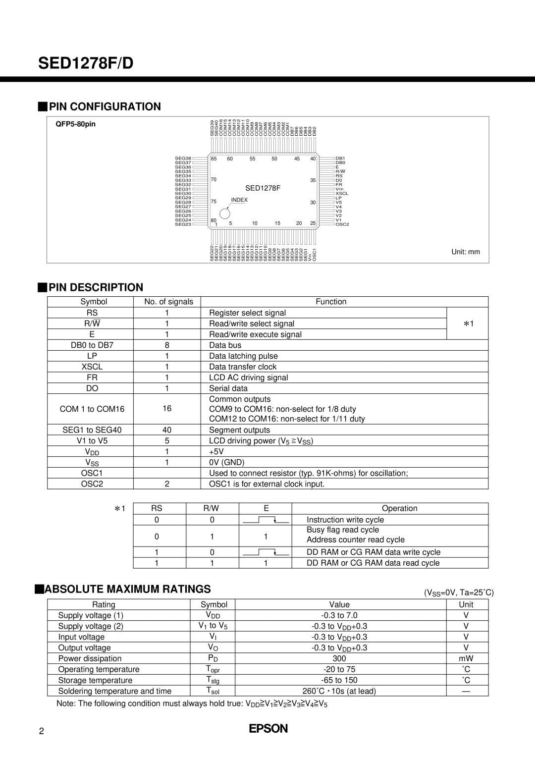
QFP5-80pin
SEG38 ![]()
SEG37 ![]()
SEG36 ![]()
SEG35 ![]()
SEG34 ![]()
SEG33 ![]()
SEG32 ![]()
SEG31 ![]()
SEG30 ![]()
SEG29 ![]()
SEG28 ![]()
SEG27 ![]()
SEG26 ![]()
SEG25 ![]()
SEG24 ![]()
SEG23 ![]()
SEG39 SEG40 | COM16 | COM15 | COM14 | COM13 | COM12 COM11 COM10 COM9 COM8 | COM7 COM6 COM5 COM4 COM3 COM2 | COM1 DB7 DB6 DB5 DB4 DB3 DB2 | ||||||||||||||||||||||||||||||||
65 |
|
| 60 |
| 55 |
| 50 |
|
|
| 45 |
|
|
| 40 | ||||||||||||||||||||||||
70 |
|
|
|
|
|
|
|
|
|
|
|
|
|
|
|
|
|
|
|
|
|
|
|
|
|
|
|
|
|
|
|
|
|
|
| 35 | |||
|
|
|
|
|
|
|
| SED1278F |
|
|
|
|
|
|
|
|
|
|
|
|
|
| |||||||||||||||||
75 |
|
| INDEX |
|
|
|
|
|
|
|
|
|
|
|
|
|
|
|
|
|
|
|
|
|
| 30 | |||||||||||||
|
|
|
|
|
|
|
|
|
|
|
|
|
|
|
|
|
|
|
|
|
|
|
|
|
|
|
|
|
|
|
|
|
|
| |||||
80 |
|
| 5 |
| 10 | 15 |
|
| 20 |
|
| 25 | |||||||||||||||||||||||||||
1 |
|
|
|
|
|
|
| ||||||||||||||||||||||||||||||||
|
|
|
|
|
|
|
|
|
|
|
|
|
|
|
|
|
|
|
|
|
|
|
|
|
|
|
|
|
|
|
|
|
|
|
|
|
|
| |
|
|
|
|
|
|
|
|
|
|
|
|
|
|
|
|
|
|
|
|
|
|
|
|
|
|
|
|
|
|
|
|
|
|
|
|
|
|
|
|
SEG22 SEG21 | SEG20 | SEG19 | SEG18 | SEG17 | SEG16 SEG15 SEG14 SEG13 SEG12 | SEG11 SEG10 SEG9 SEG8 SEG7 SEG6 | SEG5 SEG4 SEG3 SEG2 SEG1 | VSS OSC1 | |||||||||||||||||||||||||||||||
DB1
DB0
E R/W
RS
D0
FR
VDD XSCL LP V5 V4 V3 V2 V1 OSC2
Unit: mm
 PIN DESCRIPTION
Symbol | No. of signals | Function | ||
RS | 1 | Register select signal | ||
|
|
| 1 | Read/write select signal |
R/W |
| |||
E | 1 | Read/write execute signal | ||
DB0 to DB7 | 8 | Data bus | ||
LP | 1 | Data latching pulse | ||
XSCL | 1 | Data transfer clock | ||
FR | 1 | LCD AC driving signal | ||
DO | 1 | Serial data | ||
|
|
| 16 | Common outputs |
COM 1 to COM16 | COM9 to COM16: | |||
|
|
|
| COM12 to COM16: |
SEG1 to SEG40 | 40 | Segment outputs | ||
V1 to V5 | 5 | > | ||
LCD driving power (V5 = VSS) | ||||
VDD | 1 | +5V | ||
VSS | 1 | 0V (GND) | ||
OSC1 |
| Used to connect resistor (typ. | ||
OSC2 | 2 | OSC1 is for external clock input. | ||
![]() 1
1
![]() 1
1
RS | R/W |
|
| E | Operation | ||
|
|
|
|
|
|
|
|
0 | 0 |
|
|
|
|
| Instruction write cycle |
|
|
|
|
| |||
|
|
|
|
|
|
|
|
0 | 1 | 1 |
|
| Busy flag read cycle | ||
|
| Address counter read cycle | |||||
|
|
|
|
|
|
| |
|
|
|
|
|
|
|
|
1 | 0 |
|
|
|
|
| DD RAM or CG RAM data write cycle |
|
|
|
|
| |||
|
|
|
|
|
|
|
|
1 | 1 | 1 |
|
| DD RAM or CG RAM data read cycle | ||
| ABSOLUTE MAXIMUM RATINGS |
| (VSS=0V, Ta=25˚C) | ||||
|
|
|
|
| |||
|
| Rating | Symbol | Value |
| Unit |
|
|
| Supply voltage (1) | VDD |
| V |
| |
|
| Supply voltage (2) | V1 to V5 |
| V |
| |
|
| Input voltage | VI |
| V |
| |
|
| Output voltage | VO |
| V |
| |
|
| Power dissipation | PD | 300 |
| mW |
|
|
| Operating temperature | Topr |
| ˚C |
| |
|
| Storage temperature | Tstg |
| ˚C |
| |
|
| Soldering temperature and time | Tsol | 260˚C 10s (at lead) |
| — |
|
|
|
|
| > > > > > |
|
|
|
|
| Note: The following condition must always hold true: VDD=V1=V2=V3=V4=V5 |
|
|
| ||
2