SED1278F/D
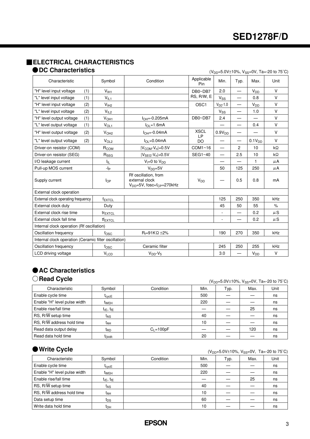
 ELECTRICAL CHARACTERISTICS DC Characteristics
(VDD=5.0V±10%, VSS=0V,
Characteristic |
| Symbol | Condition | Applicable | Min. | Typ. | Max. | Unit | |
| Pin | ||||||||
|
|
|
|
|
|
|
| ||
|
|
|
|
|
|
|
|
| |
"H" level input voltage | (1) | VIH1 |
| DB0~DB7 | 2.0 | — | VDD | V | |
"L" level input voltage | (1) | VIL1 |
| RS, R/W, E | VSS | — | 0.8 | V | |
|
| ||||||||
"H" level input voltage | (2) | VIH2 |
| OSC1 | — | VDD | V | ||
"L" level input voltage | (2) | VIL2 |
|
| VSS | — | 1.0 | V | |
"H" level output voltage | (1) | VOH1 | DB0~DB7 | 2.4 | — | — | V | ||
"L" level output voltage | (1) | VOL1 | IOL=1.6mA |
| — | — | 0.4 | V | |
"H" level output voltage | (2) | VOH2 | XSCL | 0.9VDD | — | — | V | ||
|
|
|
| LP |
|
|
|
| |
"L" level output voltage | (2) | VOL2 | IOL=0.04mA | — | — | 0.1VDD | V | ||
DO | |||||||||
| RCOM | COM1~16 | — | 2 | 10 | k | |||
| RSEG | SEG1~40 | — | 2.5 | 10 | k | |||
I/O leakage current |
| IIL | VI=0 to VDD |
| — | — | 1 | A | |
| VDD=5V |
| 50 | 125 | 250 | A | |||
|
|
| Rf oscillation, from |
|
|
|
|
| |
Supply current |
| IOP | external clock | VDD | — | 0.5 | 0.8 | mA | |
|
|
| VDD=5V, fosc=fCP=270kHz |
|
|
|
|
| |
External clock operation |
|
|
|
|
|
|
|
| |
|
|
|
|
|
|
|
| ||
External clock operating frequency | fEXTCL |
|
| 125 | 250 | 350 | kHz | ||
External clock duty |
| Duty |
|
| 45 | 50 | 55 | % | |
|
|
|
|
|
|
|
|
| |
External clock rise time |
| trEXTCL |
|
| - | — | 0.2 | S | |
External clock fall time |
| tfEXTCL |
|
| - | — | 0.2 | S | |
Internal clock operation (Rf oscillation)
Oscillation frequency
fOSC
Rf=91K ±2%
190
270
350
kHz
Internal clock operation (Ceramic filter oscillation)
Oscillation frequency | fOSC | Ceramic filter |
| 245 | 250 | 255 | kHz |
LCD driving voltage | VLCD |
| 3.0 | — | VDD | V |
 AC Characteristics
  Read Cycle
(VDD=5.0V±10%, VSS=0V,
| Characteristic | Symbol | Condition | Min. | Typ. | Max. | Unit | |
|
|
|
|
|
|
|
|
|
Enable cycle time | tcycE |
| 500 | — | — | ns | ||
Enable "H" level pulse width | tWEH |
| 220 | — | — | ns | ||
Enable rise/fall time | trE, tfE |
| — | — | 25 | ns | ||
|
|
| tAS |
|
|
|
|
|
RS, R/W | setup time |
| 40 | — | — | ns | ||
|
|
| tAH |
|
|
|
|
|
RS, R/W | address hold time |
| 10 | — | — | ns | ||
Read data output delay | tRD | CL=100pF | — | — | 120 | ns | ||
Read data hold time | tDHR |
| 20 | — | — | ns | ||
Write Cycle
(VDD=5.0V±10%, VSS=0V,
| Characteristic | Symbol | Condition | Min. | Typ. | Max. | Unit | |
|
|
|
|
|
|
|
|
|
Enable cycle time | tcycE |
| 500 | — | — | ns | ||
Enable "H" level pulse width | tWEH |
| 220 | — | — | ns | ||
Enable rise/fall time | trE, tfE |
| — | — | 25 | ns | ||
|
|
| tAS |
|
|
|
|
|
RS, R/W | setup time |
| 40 | — | — | ns | ||
|
|
| tAH |
|
|
|
|
|
RS, R/W | address hold time |
| 10 | — | — | ns | ||
Data setup time | tDS |
| 60 | — | — | ns | ||
Write data hold time | tDH |
| 10 | — | — | ns | ||
3
