PRELIMINARY
REFERENCE B
Introduction to LVDS
National Semiconductor first introduced LVDS as a standard in 1994. National recognized that the demand for bandwidth was increasing at an exponential rate while users also desired low power dissipation. This exceeded the speed capabilities of
LVDS is differential, using two signal lines to convey information. While sounding like a penalty, this is actually a benefit. The cost is two traces (or conductors) to convey a signal, but the gain is noise tolerance in the form of
Signal swing can be dropped to only a few hundred millivolts because the
Getting Speed with Low Noise and Low Power
LVDS is a low swing, differential signaling technology, which allows single channel data transmission at hundreds or even thousands of Megabits per second (Mbps). Its low swing and
How LVDS Works
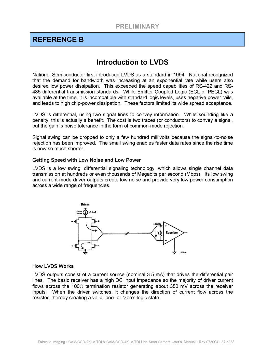
LVDS outputs consist of a current source (nominal 3.5 mA) that drives the differential pair lines. The basic receiver has a high DC input impedance so the majority of driver current flows across the 100Ω termination resistor generating about 350 mV across the receiver inputs. When the driver switches, it changes the direction of current flow across the resistor, thereby creating a valid “one” or “zero” logic state.
Fairchild Imaging •
