July 2003
FDD6690A
FDD6690A
30V N-Channel PowerTrench® MOSFET
General Description
This
Applications
∙DC/DC converter
∙Motor Drives
Features
∙46 A, 30 V RDS(ON) = 12 mΩ @ VGS = 10 V RDS(ON) = 14 mΩ @ VGS = 4.5 V
∙Low gate charge
∙Fast Switching Speed
∙High performance trench technology for extremely
low RDS(ON)
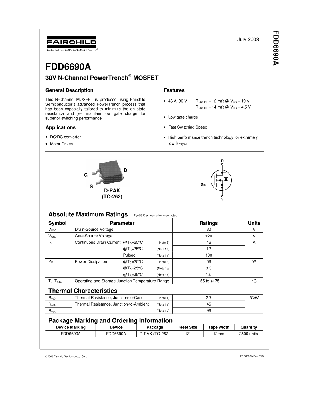
D
D
G
SG ![]()
![]()
![]()
![]()
|
|
|
|
|
|
|
|
|
|
|
|
|
|
| |
|
|
|
|
| S | ||
|
|
|
|
|
| ||
Absolute Maximum Ratings TA=25oC unless otherwise noted |
|
|
| ||||
Symbol | Parameter |
|
| Ratings |
| Units | |
VDSS |
|
|
| 30 |
| V | |
|
|
|
|
|
|
|
|
VGSS |
|
|
| ±20 |
| V | |
|
|
|
|
|
|
|
|
ID | Continuous Drain Current | @TC=25°C | (Note 3) |
| 46 |
| A |
|
| @TA=25°C | (Note 1a) |
| 12 |
|
|
|
| Pulsed | (Note 1a) |
| 100 |
|
|
|
|
|
|
|
|
|
|
PD | Power Dissipation | @TC=25°C | (Note 3) |
| 56 |
| W |
|
| @TA=25°C | (Note 1a) |
| 3.3 |
|
|
|
| @TA=25°C | (Note 1b) |
| 1.5 |
|
|
TJ, TSTG | Operating and Storage Junction Temperature Range |
|
| °C | |||
|
|
|
|
|
|
|
|
Thermal Characteristics |
|
|
|
|
|
| |
RθJC | Thermal Resistance, | (Note 1) |
| 2.7 |
| °C/W | |
RθJA | Thermal Resistance, | (Note 1a) |
| 45 |
|
| |
RθJA |
|
| (Note 1b) |
| 96 |
|
|
Package Marking and Ordering Information
Device Marking | Device | Package | Reel Size | Tape width | Quantity |
|
|
|
|
|
|
FDD6690A | FDD6690A | 13’’ | 12mm | 2500 units | |
|
|
|
|
|
|
©2003 Fairchild Semiconductor Corp. | FDD6690A Rev EW) |