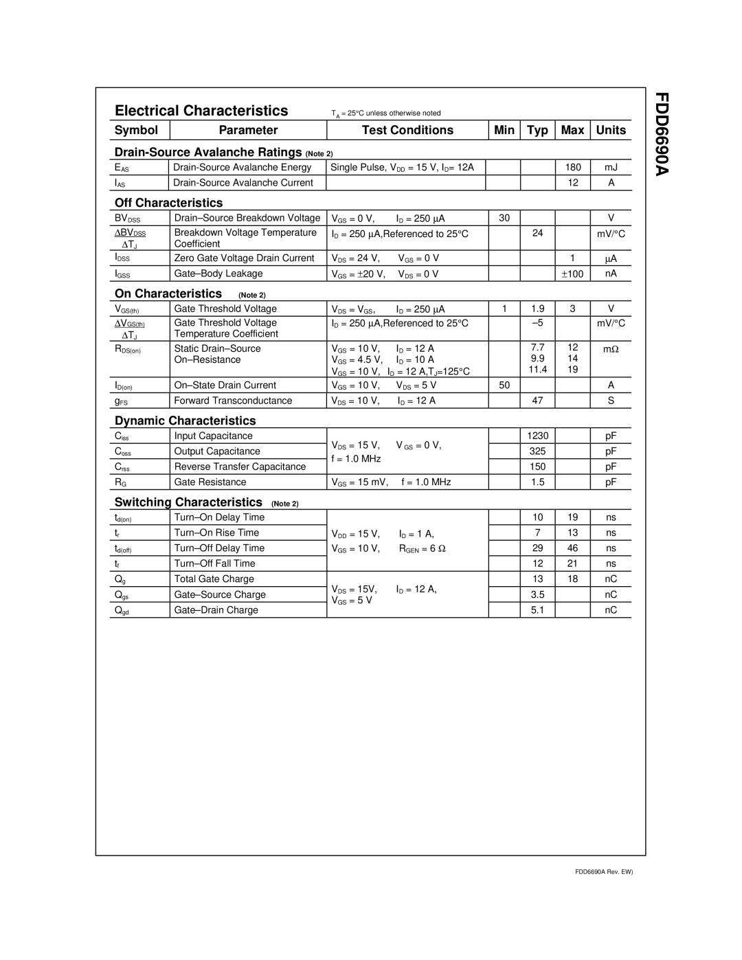
Electrical Characteristics | TA = 25°C unless otherwise noted |
|
|
|
| |||
Symbol | Parameter | Test Conditions | Min | Typ | Max | Units | ||
|
|
|
|
|
|
|
|
|
|
|
|
|
|
| |||
EAS | Single Pulse, VDD = 15 V, ID= 12A |
|
|
| 180 | mJ | ||
IAS |
|
|
|
|
| 12 | A | |
|
|
|
|
|
|
|
|
|
Off Characteristics |
|
|
|
|
|
|
| |
BVDSS | VGS = 0 V, | ID = 250 μA | 30 |
|
| V | ||
ΔBVDSS | Breakdown Voltage Temperature | μ | ° |
|
| 24 |
| ° |
ΔTJ | Coefficient | ID = 250 A,Referenced to 25 C |
|
| mV/ C | |||
|
|
|
|
|
|
| ||
IDSS | Zero Gate Voltage Drain Current | VDS = 24 V, | VGS = 0 V |
|
| 1 | μ | |
|
|
| A | |||||
IGSS | VGS = ±20 V, | VDS = 0 V |
|
| ±100 | nA | ||
On Characteristics (Note 2) |
|
|
|
|
|
|
| |
VGS(th) | Gate Threshold Voltage | VDS = VGS, | ID = 250 μA | 1 | 1.9 | 3 | V | |
ΔVGS(th) | Gate Threshold Voltage | ID = 250 μA,Referenced to 25°C |
|
| mV/°C | |||
ΔTJ | Temperature Coefficient |
|
|
|
|
|
|
|
RDS(on) | Static | VGS = 10 V, | ID = 12 A |
| 7.7 | 12 | mΩ | |
| VGS = 4.5 V, | ID = 10 A |
| 9.9 | 14 |
| ||
|
|
| ° |
|
| 11.4 | 19 |
|
|
| VGS = 10 V, ID = 12 A,TJ=125 C |
|
|
|
| ||
ID(on) | VGS = 10 V, | VDS = 5 V | 50 |
|
| A | ||
gFS | Forward Transconductance | VDS = 10 V, | ID = 12 A |
| 47 |
| S | |
Dynamic Characteristics |
|
|
|
|
|
|
| |
Ciss | Input Capacitance | VDS = 15 V, | V GS = 0 V, |
| 1230 |
| pF | |
|
|
|
|
|
| |||
Coss | Output Capacitance |
| 325 |
| pF | |||
f = 1.0 MHz |
|
|
|
| ||||
|
|
|
|
|
|
|
| |
Crss | Reverse Transfer Capacitance |
|
|
| 150 |
| pF | |
|
|
|
|
| ||||
|
|
|
|
|
|
|
| |
RG | Gate Resistance | VGS = 15 mV, | f = 1.0 MHz |
| 1.5 |
| pF | |
Switching Characteristics (Note 2) |
|
|
|
|
|
|
| |
td(on) |
|
|
|
| 10 | 19 | ns | |
|
|
|
|
|
|
|
| |
tr | VDD = 15 V, | ID = 1 A, |
| 7 | 13 | ns | ||
td(off) | VGS = 10 V, | RGEN = 6 Ω |
| 29 | 46 | ns | ||
tf |
|
|
|
| 12 | 21 | ns | |
Qg | Total Gate Charge | VDS = 15V, | ID = 12 A, |
| 13 | 18 | nC | |
Qgs |
| 3.5 |
| nC | ||||
VGS = 5 V |
|
|
|
| ||||
|
|
|
|
|
|
|
| |
Qgd |
|
|
| 5.1 |
| nC | ||
|
|
|
|
| ||||
|
|
|
|
|
|
|
|
|
FDD6690A
FDD6690A Rev. EW)