PC-CARD-DAS16/16AO User's Guide | Functional Details |
After a conversion is made, the sample is stored in a 4096-word (sample) FIFO buffer from which it may be retrieved one sample at a time or in blocks via REP-INSW transfers.
How does the FIFO size and design affect throughput?
The 4096-sample FIFO buffer stores samples from the A/D converter as they are being converted. When a block of samples is ready and when the PC is ready, the FIFO is emptied into system memory. Most FIFO designs employ a half-full transfer initiation circuit. When the FIFO is half full, the transfer request is made. Samples continue to fill the second half of the FIFO while the CPU responds to the transfer request and transfers data to system memory.
A/D pacer clock
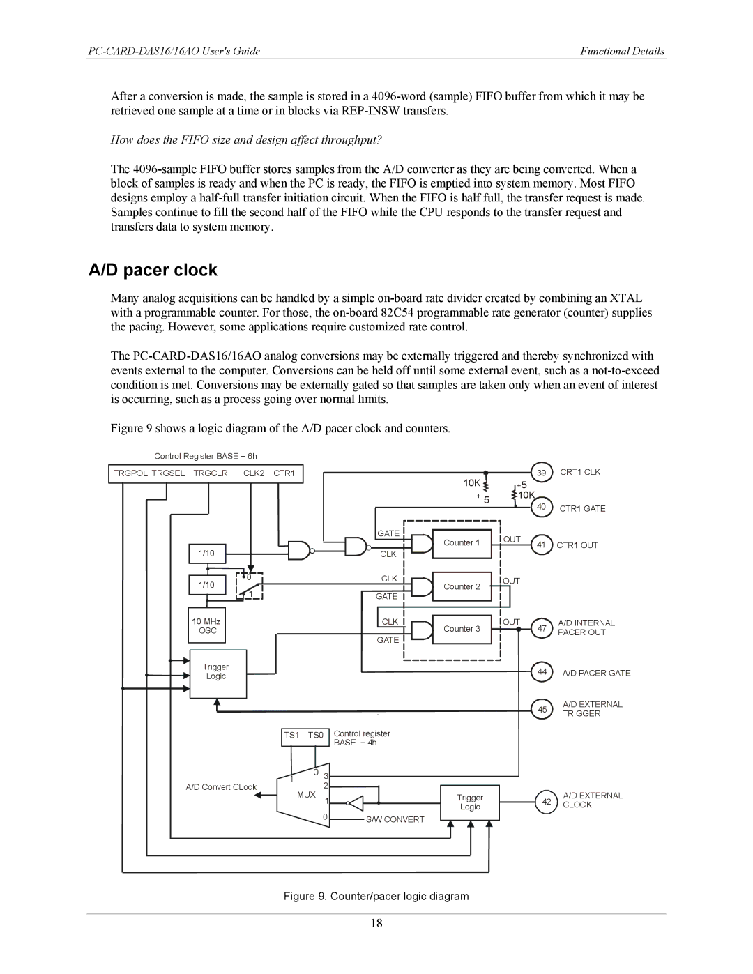
Many analog acquisitions can be handled by a simple on-board rate divider created by combining an XTAL with a programmable counter. For those, the on-board 82C54 programmable rate generator (counter) supplies the pacing. However, some applications require customized rate control.
The PC-CARD-DAS16/16AO analog conversions may be externally triggered and thereby synchronized with events external to the computer. Conversions can be held off until some external event, such as a not-to-exceed condition is met. Conversions may be externally gated so that samples are taken only when an event of interest is occurring, such as a process going over normal limits.
Figure 9 shows a logic diagram of the A/D pacer clock and counters.
Control Register BASE + 6h
TRGPOL TRGSEL | TRGCLR | CLK2 | CTR1 | | | 10K | | 5 | 39 | CRT1 CLK |
| | | | | | | | |
| | | | | | | 5 | 10K | 40 | |
| | | | | | | | CTR1 GATE |
| | | | | | | | |
| | | | | | GATE | | OUT | | |
| | | | | | Counter 1 | | 41 | CTR1 OUT |
| 1/10 | | | | | | |
| | | | | CLK | | | | |
| 1/10 | 0 | | | | CLK | | OUT | | |
| 1 | | | | Counter 2 | | | | |
| | | | | GATE | | | | |
| 10 MHz | | | | | CLK | | OUT | 47 | A/D INTERNAL |
| OSC | | | | | Counter 3 | | | PACER OUT |
| | | | | | GATE | | | | |
| Trigger | | | | | | | | 44 | A/D PACER GATE |
| Logic | | | | | | | |
| | | | | | | | | |
| | | | | | | | | 45 | A/D EXTERNAL |
| | | | | | | | | TRIGGER |
| | | | | | | | | |
| | | TS1 | TS0 | Control register | | | | |
| | | | | | BASE + 4h | | | | |
| A/D Convert CLock | 1 | 0 | 3 | | | | | |
| MUX | 2 | Trigger | | | | A/D EXTERNAL |
| | | 1 | | | 42 |
| | | | | Logic | | | CLOCK |
| | | | | 0 | | | |
| | | | | S/W CONVERT | | | | |
Figure 9. Counter/pacer logic diagram

