X25-M, X18-M specifications
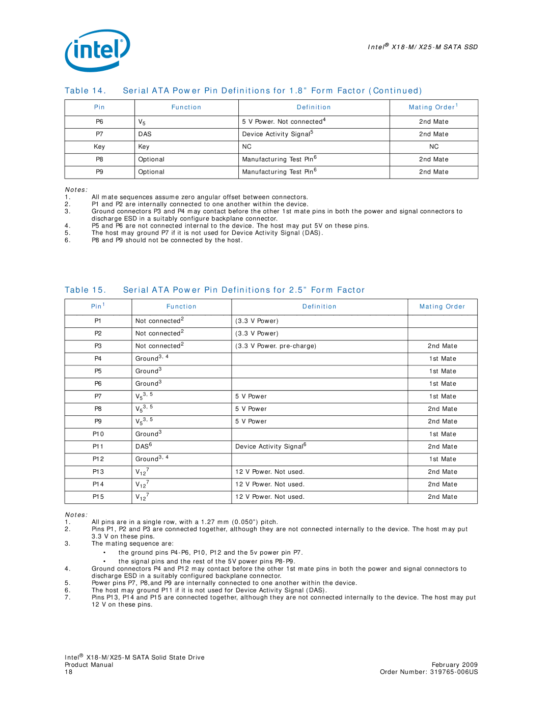
Intel has made significant strides in the realm of solid-state drives (SSDs) with its X18-M and X25-M series. Launched to cater to the growing demand for faster, more reliable storage solutions, these drives leverage cutting-edge technologies that redefine the possibilities for both consumers and businesses.The Intel X25-M, specifically designed for consumer-level computers, marked a major leap in performance compared to traditional hard disk drives. This 2.5-inch SATA SSD provides data transfer speeds that can reach up to 250 MB/s for read operations and around 70 MB/s for writes. Such numbers are commendable, especially in the context of the time of its release, offering users a substantial upgrade in boot times and application loading.
On the other hand, the X18-M is a smaller, 1.8-inch variant intended for ultra-portable laptops and devices where space is a premium. It similarly benefits from the same performance enhancing technologies as its larger counterpart. Both drives utilize Intel's proprietary NAND flash memory, optimized for durability and efficiency. With a mean time between failures (MTBF) rating of over a million hours, these SSDs promise long-lasting reliability.
A noteworthy feature of these drives is their support for the TRIM command, which actively manages unused data blocks, helping to maintain optimal performance over time. Elaborate firmware algorithms further optimize read/write cycles, thereby enhancing endurance and reducing wear.
The X series also showcases impressive power efficiency. The SSDs draw less power compared to traditional HDDs, making them ideal for mobile devices where battery life is crucial. In idle states, their power consumption can drop to just a fraction of a watt, translating to longer usage without needing a recharge.
In addition to speed and longevity, security features are also part of the package. Both the X18-M and X25-M support AES 128-bit hardware encryption, offering an additional layer of data protection, which is particularly important in environments managing sensitive information.
In conclusion, the Intel X18-M and X25-M SSDs represent a significant evolution in storage technology, combining high performance, durability, power efficiency, and enhanced security. Ideal for a range of applications from consumer laptops to enterprise-level solutions, they laid the groundwork for future advancements in solid-state storage, ushering in a new era of computing experiences.

