CIRCUIT DIAGRAMS

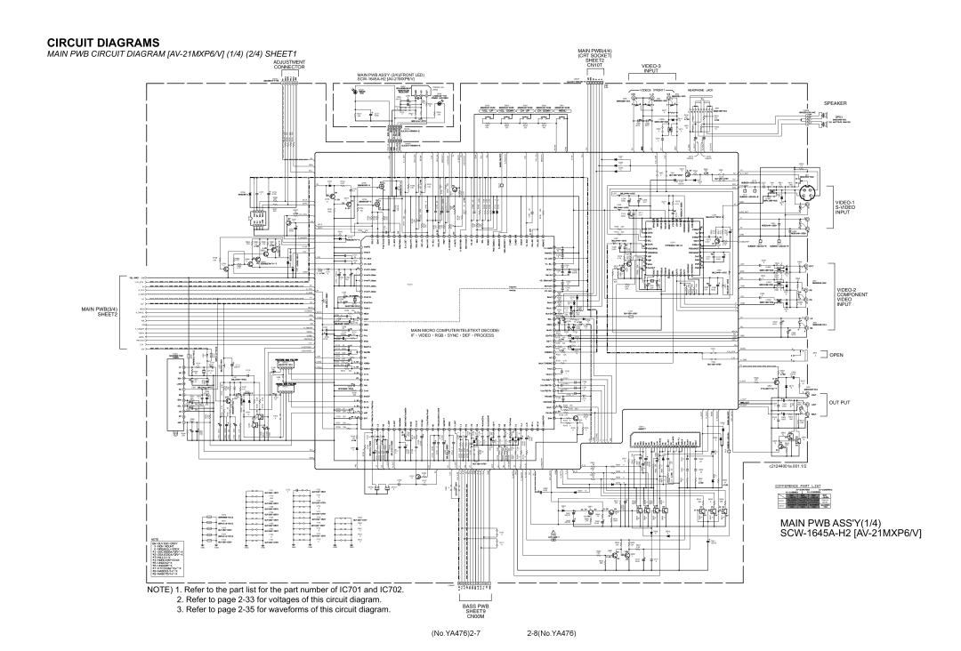
MAIN PWB CIRCUIT DIAGRAM [AV-21MXP6/V] (1/4) (2/4) SHEET1

ADJUSTMENT

CONNECTOR


MAIN PWB ASS'Y (2/4)(FRONT LED)

CN00C

SCW-1645A-H2 [AV-21MXP6/V]


IC801


POWER LED


IC302


(RED)


D808


C808

C806


X


100/16

C807

.1/16


R822


Y813


1K

S805

S804

S803

S802


X


C317

Y814

R823


R824


R327

0


470


39K

10/50


X


R825


MAIN PWB(4/4)

(CRT SOCKET)

SHEET2

CN10T

CN00T

J808

S801

VIDEO-3

INPUT

J806


J807


J809


R817


X


R630

R632


270

270


LC805

D814


*8


C825

C826


SPEAKER

CN00S


220

220

220

220


R764

R765

R762

R763

5V

SDA

ECO IN

PW LED

REMOTE

1.8V


R821

R820

R819


R818

CN10A


470

330

220


180


CN00A


S V DET

VDO DET

KEYIN

1.8V

ECO IN

PROTECT

4.5/OTHER

5V

A MUTE 5V

3.58/OTHER

SDA

SCL

PW

S REDUCE

1.8V

PW LED

REMOTE

KEYIN

GND

12V


V1.8A

12V

R3

D341

*3

D342

*3

.0015

.0015


R631


R633


Y809


1K


1K


Y810


X


X


C831


0


GND

L3

V3

GND

A GND

L AOUT

R AOUT

B MUTE


STB

3.3V

C615


C616


1000/25


1000/25


_


3.3V


R816

75

MAIN PWB(3/4)

SHEET2

GND

3.3V_STB

8V A_VCC

A_GND

5V

12V

NECK

H_DRIVE

HFB

ABL

EW

P_ON/OFF

VDRA+

VDRB-

PROTECT

3.3V

32V

TU001


D706


C777

C778


.1

47/35


R760


220


R761


220


IC702


R984

R983

R982

R981


47K

3.9

47K

3.9


*1

Q981


Q982


R796

R985

Q984


10K


4.7K

*1


Q983


Q704


*1

R986


4.7K


K103


L001

X

K101


R101


C101


10


.0047

L003


C111


220/16


C106


CF101


C110


18p

R005


X


.1


75


L101


Y008

C001


C002

10/50


6.8K

R104

180


4.7K


X

.01


L002


R107


C004


R102


D101


470/16


R001

C003


C109


2.2K

2.2K


C107

220


.1


.0047


.01

C007

56p

R002

220


2.7K


Q101


R109

R110


C008

56p


22


D102


C005


R003

3.9K


R103


R105


Y004

Q102

*5


X


0


Y003

.0022


C103.0047


C10410/50

R106100

C102.0047

R1082.2K


Q103

*5


R004


C006

33/50


C108

.0047

C105

.0047

27K


SCL


D707


R794


Q706


5V

*3


2.2K


C792


0.1


SCL0


Q708


Q707

Q705


*1


*2


SDA0


R795


R783


R976


10K


100K


1K


3.3V_STB


Q791


R759

3.3K

*1


PW


SCL0


SDA0


C793


R793

100


10/50


R790


1K


P_ON/OFF


D713


V1.8A


1.8V


C701


1.8V


.22


C702


D982


.22


D981

CONT

R792

L703

470/10


33

*4


C704

C790


C703


.1

27p


8V


A_VCC


5V


A_GND


C705


7p


5V


C706


L701


7p


12V


X701


NECK


H_DRIVE


R756

10K


NECK


HFB


C785


X


CONT


ABL


L718


C784


EW


.47/50


P_ON/OFF

C707

.1


C709


.01


VDRA+


C710

R701


VDRB-


6800p

12K


C708

C711


PROTECT

47/16

2.2/50


3.3V


C712

.22


4.5/OTHER


C713

10/50


3.58/OTHER


C714

.022


EW


R702

X


C715

.001


SF102


VDRB-


R703


100


C716


.001


VDRA+


R704

100


SF101


C718


*


R705


39K


C719

.01


R706

220


C720

.001


R707

22K


R708

10K


R709

C721

X


1M


D701

C794


SCL


*3

X


R710


SDA


D714

C775

220/16

R758

3.3K

R757

4.7K


C776

.1

1


1


C723


C724


5.6K

10K

5.6K

10K

C795

C725

.1

R711

R712

R713

R714


R755


R753


R750 10K


W-A1


R740 15K


1.2K


R789 X


1.2K


Q612

*1


R787

4.7K


*3


.22


22/50

C770 .1


.22


3.3K


3.3K

220

4.7K

*3

*3


1/50


D709


C772


C771

R747 100


1K

R744C768


R745


R743

R741

R785

D711

D712

C767 .22

R736 100

R777 100

R776

15K

C783

R754

220

R752

100

R751

100

R749

1K

R748

2.7K

R771

220

R742

220

IC701

*

MAIN MICRO COMPUTER/TELETEXT DECODE/

IF VIDEO RGB SYNC DEF PROCESS

C727

3300p


1


C782 1

R738

100

C736

.01

C744

.1


R737

100


C739

1

R739

100

D710

*8


R715

390

C729

2.2/50


C732

2.2/50

C781


D702

*8

C745

.1

C737

.1

C738

1

C740

.1

C743

10/50

C742

10/50

C726

10/50

C728

.1


C730 22/50

C731 .1

L702

C734 .1

R772 5.6K

R773 10K

5.6K

R775 10K

C735 .1


R786

75


D703

*8


5.6K


R717 10K

R718 5.6K

10K

R768 D704

*8

R769 C741

.1


R774


R716


R719

100

0

R770

0


Y707


C766

.22

C764

X


C763


X


C761


C762


.1


100/16


C760


.22


C758


.22


R735


100


R734


D715


100


*3


R733


D716


100


*3


D717


R720


R732


68K


*3


1K


C717


R721


C757


1/50


47K


560p


C756

R731

D708


1K

*3


.1


C755

L706


10/50

*4


C779


C753

C754


10/50


.1


.1


R779

100


D753


*8


R780

100

C752

.1


C751

.1


R781

100


D751


R782

1.2K


*8


R729

4.7K


C780


.1


C750.1


C786


C749.1


X


C787


C748.1


X


C788 X


C746


L716


.1


*4


R728

100


R727

560


R726

27K


R725


X


R724

X


Q702


X


R778

X


R722


R723


X


X


5V

HFB

H_DRIVE

V

U

Y

D343


*3


L301


C304


10/50


L305


C310


10/50


R309

220


R312

220


L302


C306


C307

0.01

10/50


4.7K


R311

4.7K

R310


R314


*1

Q305


22K


Q306

*1


R313


82K


R307

22K

K701

ABL


10K

R617

R618

X

C305

0.01

C311

0.01

C318

27p

X301

R308 33K

C302

27P

IC601

Q341

*2

Y942

Y941

X


C341

100/16

D301

R319

*3

4.7K


C314


IC301

27P


C303

10K


R317

C602

10/50

D602

X

C611 X

R344

22

D345

*3

10K

10K

R316

R315

L_AOUT

C605

.22

R961

10KY909C1 X

5V S_V_DET

Y912


12V


SCL


Y1/CVBS1


SDA


W-C


GND


5V


VDO_DET


L304


L1


R1

R320

3.3K

R321

4.7K

C316

100/16

GND

C315


0.047


R318

CVBSO/PIP


Q307

4.7K


*2


C313 C312

0.0110/50


V2/Y


L306

GND


PB

C309

C308

L303

GND

0.01

10/50


PR


V

GND


Y


U


L2


R2


NECK


PB

GND


GND


V2/Y


PR


Y943


BASS

X3.3V_STB

3.3V

A_GND

Y944

5V

V_OUT

L_OUT

GND

R_OUT

R AOUT

BASS

S REDUCE

OFF MUTE


D605


X


D604


X


C614

X

W-A


J801


W-C1


C827

Y801

R801

Y819


0

X


75

BW


Y802


X


LC801


D817


*8


C821


C822


W-G

W-G1


C828


R804


0

Y803

X


75


LC802


Y804

D810


C829

X *8


0

Y805

X

R805


LC803


75

J802


Y806

X


D811


C830


*8


0


LC804


R806


75


D812


*8


C823


J803


.0015


C824


.0015


J805


X


R807

C804


100


470/16


R809


220


R815


75


Q801


D813

J804


*8


C809


R810 390

R811


X


C802

82K


10/50


C810


C803

R812


X


10/50

390

R813


82K


Q803


*6


Q804


Q805


*6


*2


R814


100K


VIDEO-1

S-VIDEO

INPUT

VIDEO-2

COMPONENT VIDEO INPUT

OPEN

OUT PUT

ABL

L3

R3

L OUT

R OUT

8V

5V

V OUT

L1

R1

V3

V2/Y

L2

R2

Y1/CVBS1

C1

A L

A R

CVBSO/PIP


R601

P_R

3K

R637 0

10K

X

C603 .22

c21244001a.001.1/2

C722

R767

5V

3.3V

3.3VSTB

A L

A R

12V

SCL

SDA

GND

A B

P R

P L

GND

BMUTE

GND

ON/OFFP

A VCC

12V

5V

OFFMUTE


R766


X


Q701


X


X

X


GND

MUTE

P L

A_B

X


R602


A_


3K

R638 X

R639 0

D610 *3

R604

R605


C604

.22

C612 X


R619

X

R606

2.2

R625 X

C606

.22

R607

2.2

D606

X


R640

1K


CF702

CF701


Y711

C773

Y722


X

X


.1


Y710


Y721


BW


X


Y709


Y720


Y708


Y718


X


Y706


Y717


K702


Y705


Y716


Y968


K651


Y704


Y715


Y962


X


K105


Y703


Y714


Y961


X


X


K104


Y702


Y713


Y824


X


X


K102


Y101


Y712


Y812


X


X


GND

GND

GND

GND

GND

GND

GND

GND


NOTE) 1. Refer to the part list for the part number of IC701 and IC702.

2.Refer to page 2-33 for voltages of this circuit diagram.

3.Refer to page 2-35 for waveforms of this circuit diagram.

Y963

X

Y964

Y610

X

Y611

X

CN00M

BASS PWB

SHEET9

CN00M

C662


10/50

D607

*3


10K

R612 100K

R613 X

R614 100K

R615 X


R611

100/16


D603


Q601


C610


*3


*2


C607


Q602


R649

*2


220/16


Q603 *6

Q604 X

Q605 *6

Q606 X


1K


R609


R610


C608


27K

C609

100K


220/16


33/50


!


D608

D609


X

X

CP650


R623

R620


33K

10K

R621


2.2K


R622

Q607


10K

*1

Q608


*1


C613


C617


R624


10/50


X


68K


R634

R635

R636

390

X

390

Q609 *6

Q610 X

Q611 *6


C661


100/16


IC701

Refer to


NOTE

SF101


MAIN PWB ASS'Y(1/4) SCW-1645A-H2 [AV-21MXP6/V]

(No.YA476)2-72-8(No.YA476)

Page 49
Image 49
JVC AV-25MXP6/V, AV-29MXP6/V service manual Main PWB Circuit Diagram AV-21MXP6/V 1/4 2/4 SHEET1, No.YA4762-72-8No.YA476

AV-29MXP6/V, AV-21MXP6/V, AV-25MXP6/V specifications

The JVC AV-25MXP6/V, AV-21MXP6/V, and AV-29MXP6/V are a trio of high-performance CRT televisions that represent a combination of cutting-edge technology and practical design, catering to the diverse needs of home entertainment enthusiasts. These models are characterized by their impressive picture quality, robust build, and user-friendly features, making them a prominent choice during their production era.

One of the key features of these models is their screen sizes, which cater to different room sizes and viewing preferences. The AV-25MXP6/V offers a compact 25-inch display, ideal for smaller living spaces or bedrooms, while the AV-21MXP6/V with its 21-inch screen is perfect for desk setups or as a secondary television. The AV-29MXP6/V, on the other hand, boasts a larger 29-inch display, making it suitable for home theaters or larger family rooms.

JVC is renowned for its superior picture technology, and these models are no exception. They utilize a high-quality CRT screen that provides deep contrast, vivid colors, and sharp details. The picture performance is further enhanced by JVC's proprietary circuitry, including a dynamic contrast system that adjusts brightness and contrast levels based on the content being displayed, resulting in a more immersive viewing experience.

Moreover, these televisions come equipped with several input options, including RF, composite, and S-video inputs, allowing users to connect multiple external devices such as DVD players, game consoles, and VCRs. With built-in tuners, viewers can easily access over-the-air broadcasting, making these models versatile entertainment hubs.

Another noteworthy characteristic is the user-friendly interface that JVC has engineered into the AV-25MXP6/V, AV-21MXP6/V, and AV-29MXP6/V models. The on-screen menu provides quick access to settings and customization options, allowing users to tailor the viewing experience to their preferences, including the ability to adjust color tones and picture settings.

In addition to their functionality, these televisions also sport an elegant design that incorporates a sleek frame and aesthetically pleasing finish, making them a suitable complement to any home décor.

Overall, the JVC AV-25MXP6/V, AV-21MXP6/V, and AV-29MXP6/V models represent a harmonious blend of technology, style, and user-centric features, making them reliable choices for anyone seeking quality CRT televisions for their home entertainment needs. Though newer technologies have since emerged, these models remain a fond memory for many who experienced their remarkable performance.