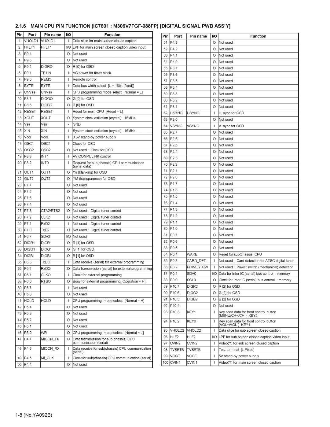
HD-52Z575 specifications
The JVC HD-52Z575, HD-61Z585, HD-61Z575, and HD-52Z585 are high-definition rear-projection televisions that were part of JVC's impressive line-up in the early 2000s. These models showcased the brand's commitment to providing quality home theater experiences with advanced features and technologies.One of the standout characteristics of these models is their use of D-ILA (Direct-Drive Image Light Amplifier) technology. D-ILA is a type of liquid crystal display technology similar to LCoS (Liquid Crystal on Silicon) that enhances picture quality by delivering deeper blacks and more vibrant colors. This technology enables the TVs to produce stunning visuals with impressive contrast ratios, making them ideal for various viewing environments.
These models are available in different screen sizes, with HD-52Z575 and HD-52Z585 featuring 52-inch screens, while the HD-61Z585 and HD-61Z575 boast larger 61-inch displays. This range offers versatility for consumers, catering to different room sizes and viewing preferences.
All four models support 1080p resolution, providing an exceptional level of detail and clarity for HD content. This feature makes them suitable for viewing high-definition broadcasts, Blu-ray films, and gaming, allowing users to immerse themselves in their favorite content. The screens also feature a wide viewing angle, ensuring that everyone in the room gets a good view without compromising picture quality.
Connectivity is another strength of these JVC models. Equipped with multiple HDMI ports, component video inputs, and composite inputs, these televisions provide compatibility with a wide range of devices, from gaming consoles to DVD players. Users can easily connect their favorite devices, expanding their entertainment options.
In terms of audio, these JVC TVs are built to complement their visual capabilities, featuring integrated speakers that deliver decent sound quality for everyday use. For those who seek an enhanced audio experience, they offer optical digital audio outputs for external sound systems.
In conclusion, the JVC HD-52Z575, HD-61Z585, HD-61Z575, and HD-52Z585 are notable for their advanced display technologies, high-definition resolutions, and versatile connectivity options. Their D-ILA technology ensures a superior viewing experience, making these rear-projection TVs a compelling choice for any home theater enthusiast looking to enjoy high-quality visuals and sound. Although released in the early 2000s, these models remain a testament to JVC's dedication to innovation and excellence in the television market.
