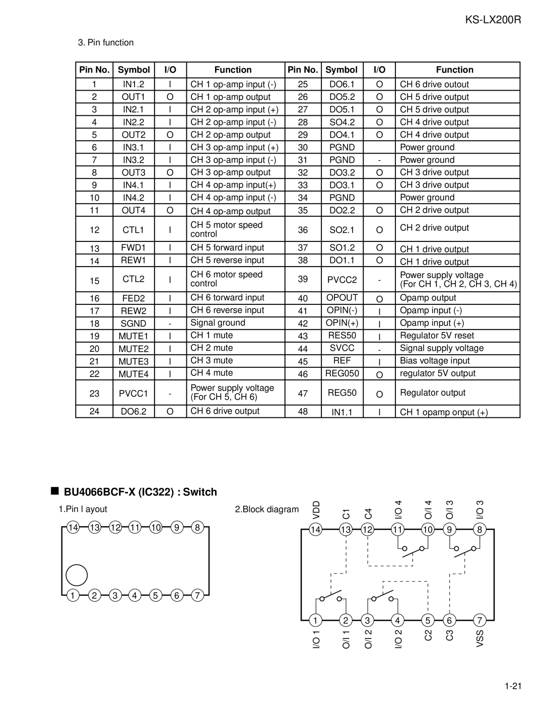
KS-LX200R specifications
The JVC KS-LX200R is a versatile car audio receiver that combines advanced technology with user-friendly features, ensuring an elevated listening experience for audiophiles and casual listeners alike. This model is celebrated for its sleek design and powerful performance, making it an ideal addition to any vehicle.One of the standout features of the KS-LX200R is its high-performance audio technology. It boasts a built-in amplifier capable of delivering up to 50 watts per channel, producing crystal-clear sound with minimal distortion. The unit supports various digital audio formats, allowing for compatibility with a wide range of media sources. Additionally, the receiver is equipped with a 13-band equalizer, enabling users to fine-tune the audio output to match their personal preferences and optimize sound quality according to the car’s acoustics.
Connectivity is at the forefront of the KS-LX200R's design. It features Bluetooth technology for hands-free calling and seamless wireless audio streaming from smartphones and other Bluetooth-enabled devices. The ability to pair multiple devices ensures that passengers can easily share their favorite music without tedious reconnections. Furthermore, the receiver includes USB and AUX inputs, giving users additional options for connecting their devices.
The KS-LX200R also accommodates various media formats, including CD, MP3, and WMA playback, ensuring that users can enjoy their entire library of audio content. The convenient front-facing USB port supports charging while listening, making it practical for long drives.
In terms of visual appeal, the KS-LX200R features a vibrant LCD display that provides clear visibility of track information and settings, even in bright sunlight. The user interface is intuitively designed, allowing quick access to various functions and settings, enhancing the overall user experience.
Moreover, the JVC KS-LX200R is built with durability in mind. It is designed to withstand the rigors of daily use in a vehicle environment while maintaining optimal performance. The receiver is compatible with steering wheel control interfaces, enabling users to operate the unit without taking their hands off the wheel for added safety.
Overall, the JVC KS-LX200R stands out as a feature-rich car audio receiver that seamlessly blends quality sound, modern convenience, and robust build quality, making it an excellent choice for any automotive sound system upgrade.

