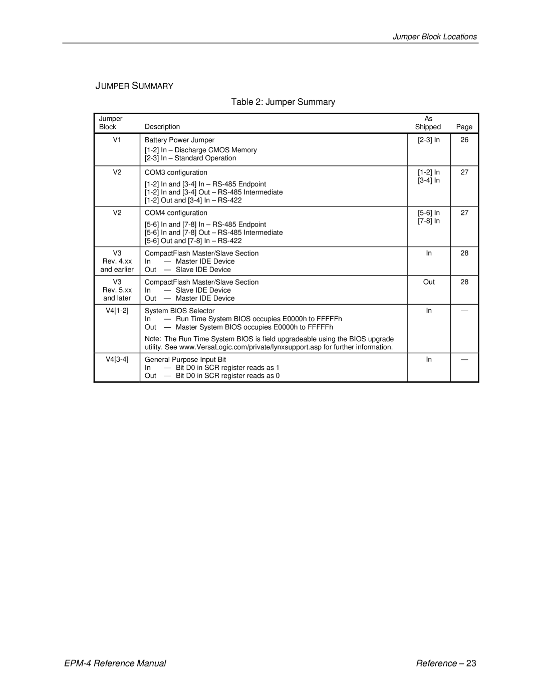
EPM-4 specifications
The Lynx EPM-4 is a cutting-edge electronic monitoring device designed for a wide range of applications including transportation, logistics, and outdoor activities. With its sleek design and robust capabilities, the EPM-4 provides users with advanced tracking and monitoring features that enhance efficiency and safety.One of the standout features of the Lynx EPM-4 is its high-precision GPS tracking technology. This allows for real-time location monitoring, ensuring that users can keep tabs on their assets or personnel at all times. The GPS functionality is complemented by cellular connectivity, enabling seamless communication and data transmission even in remote areas. Whether used in urban settings or off-the-grid locations, the EPM-4 maintains reliability and performance.
Another key characteristic of the Lynx EPM-4 is its user-friendly interface. The device is equipped with a bright LED display that provides instant access to essential information, including speed, distance traveled, and battery status. Its intuitive navigation system ensures that even users with minimal technical expertise can operate the device effectively.
Durability is a fundamental aspect of the Lynx EPM-4 design. Constructed to withstand harsh environmental conditions, it features IP67-rated water and dust resistance. This ensures that the device can perform flawlessly in diverse weather conditions, making it suitable for outdoor enthusiasts and professionals alike.
The EPM-4 also incorporates advanced battery technology, allowing for extended usage time on a single charge. This is particularly advantageous for long-haul trips or field operations where charging facilities may be unavailable. Additionally, the device supports various power management modes that optimize battery life based on usage patterns.
Connectivity options are another highlight of the Lynx EPM-4. It supports Bluetooth and Wi-Fi, enabling quick data transfer to smartphones, tablets, or computers for further analysis. Users can easily share information with team members or stakeholders, enhancing collaboration and decision-making processes.
Lastly, the Lynx EPM-4 features customizable settings, allowing users to tailor the device’s functionality to meet their specific needs. Whether it’s setting geofences, receiving alerts for unusual activity, or customizing data logging intervals, the EPM-4 ensures a personalized experience that maximizes utility.
In conclusion, the Lynx EPM-4 stands out as a premier electronic monitoring solution, combining GPS precision, robust durability, extended battery life, and versatile connectivity. With its advanced features and user-friendly design, it serves a vital role in managing logistics, ensuring safety, and enhancing operational efficiency across various industries.
