Dual, 65Msps, 14-Bit, IF/Baseband ADC
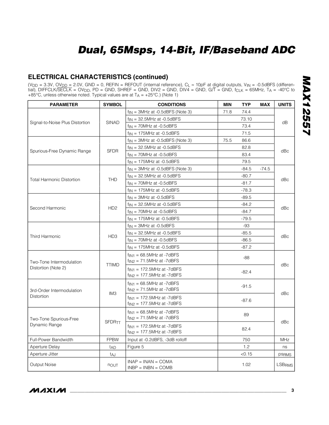
ELECTRICAL CHARACTERISTICS (continued)
(VDD = 3.3V, OVDD = 2.0V, GND = 0, REFIN = REFOUT (internal reference), CL ≈ 10pF at digital outputs, VIN =
+85°C, unless otherwise noted. Typical values are at TA = +25°C.) (Note 1)
PARAMETER | SYMBOL | CONDITIONS | MIN | TYP | MAX | UNITS |
|
|
|
|
|
|
|
|
| fIN = 3MHz at | 71.8 | 74.4 |
|
|
SINAD | fIN = 32.5MHz at |
| 73.10 |
| dB | |
fIN = 70MHz at |
| 73.4 |
| |||
|
|
|
|
| ||
|
| fIN = 175MHz at |
| 71.5 |
|
|
|
| fIN = 3MHz at | 75.5 | 86.6 |
|
|
SFDR | fIN = 32.5MHz at |
| 82.8 |
| dBc | |
fIN = 70MHz at |
| 83.4 |
| |||
|
|
|
|
| ||
|
| fIN = 175MHz at |
| 79.5 |
|
|
|
| fIN = 3MHz at |
|
| ||
Total Harmonic Distortion | THD | fIN = 32.5MHz at |
|
| dBc | |
fIN = 70MHz at |
|
| ||||
|
|
|
|
| ||
|
| fIN = 175MHz at |
|
|
| |
|
| fIN = 3MHz at |
|
|
| |
Second Harmonic | HD2 | fIN = 32.5MHz at |
|
| dBc | |
fIN = 70MHz at |
|
| ||||
|
|
|
|
| ||
|
| fIN = 175MHz at |
|
|
| |
|
| fIN = 3MHz at |
|
|
| |
Third Harmonic | HD3 | fIN = 32.5MHz at |
|
| dBc | |
fIN = 70MHz at |
|
| ||||
|
|
|
|
| ||
|
| fIN = 175MHz at |
|
|
| |
|
| fIN1 = 68.5MHz at |
|
|
| |
| fIN2 = 71.5MHz at |
|
|
| ||
TTIMD |
|
|
| dBc | ||
Distortion (Note 2) | fIN1 = 172.5MHz at |
|
| |||
|
|
|
| |||
|
|
|
|
| ||
|
| fIN2 = 177.5MHz at |
|
|
| |
|
|
|
|
|
| |
|
| fIN1 = 68.5MHz at |
|
|
| |
| fIN2 = 71.5MHz at |
|
|
| ||
IM3 |
|
|
| dBc | ||
Distortion | fIN1 = 172.5MHz at |
|
| |||
|
|
|
| |||
|
|
|
|
| ||
|
| fIN2 = 177.5MHz at |
|
|
| |
|
|
|
|
|
| |
|
| fIN1 = 68.5MHz at |
| 89 |
|
|
| fIN2 = 71.5MHz at |
|
|
| ||
SFDRTT |
|
|
| dBc | ||
Dynamic Range | fIN1 = 172.5MHz at |
| 82.4 |
| ||
|
|
|
| |||
|
|
|
|
| ||
|
| fIN2 = 177.5MHz at |
|
|
| |
|
|
|
|
|
| |
FPBW | Input at |
| 750 |
| MHz | |
|
|
|
|
|
|
|
Aperture Delay | tAD | Figure 5 |
| 1.2 |
| ns |
Aperture Jitter | tAJ |
|
| <0.15 |
| psRMS |
Output Noise | nOUT | INAP = INAN = COMA |
| 1.02 |
| LSBRMS |
INBP = INBN = COMB |
|
| ||||
|
|
|
|
|
| |
|
|
|
|
|
|
|
MAX12557
_______________________________________________________________________________________ 3