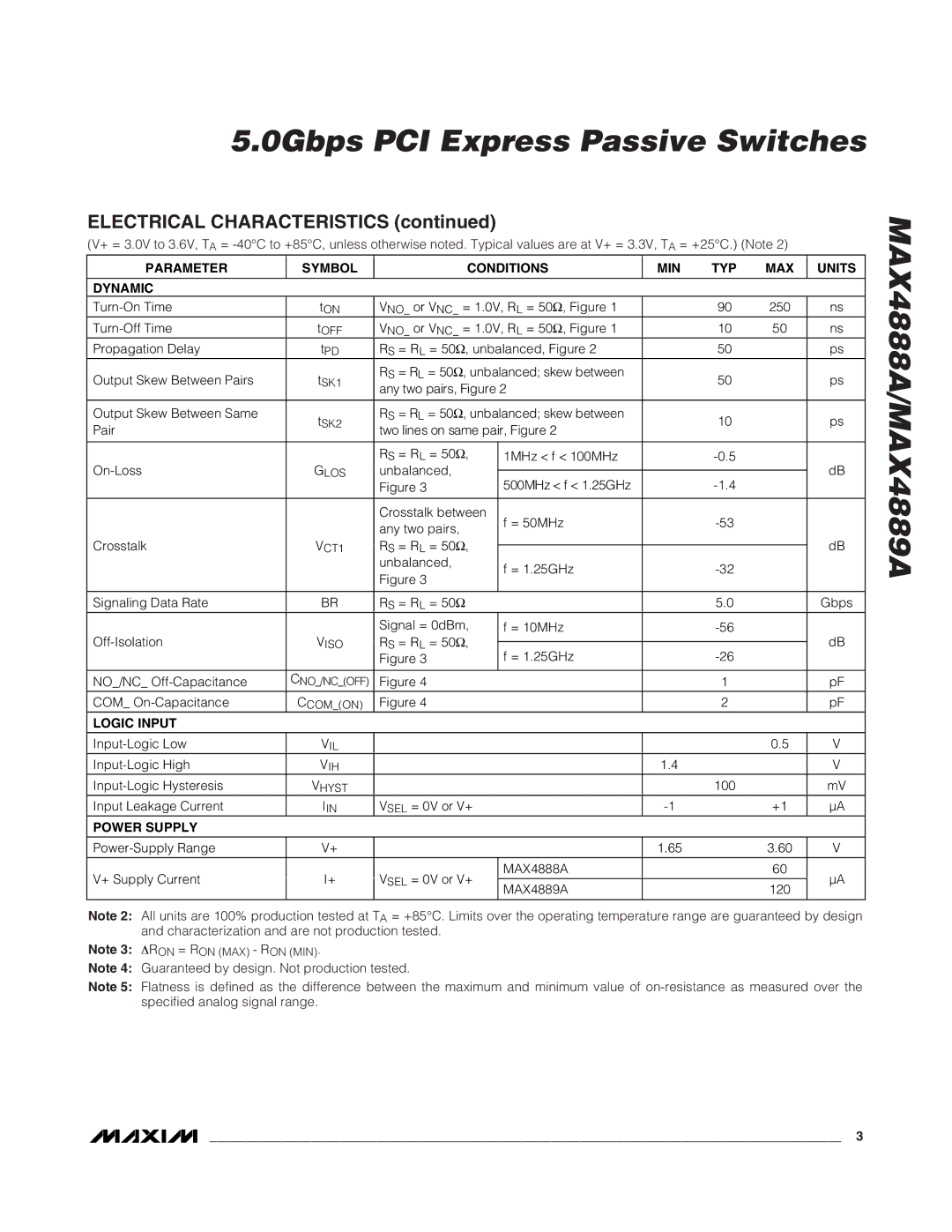
5.0Gbps PCI Express Passive Switches
ELECTRICAL CHARACTERISTICS (continued)
(V+ = 3.0V to 3.6V, TA =
PARAMETER |
| SYMBOL |
| CONDITIONS |
| MIN | TYP | MAX |
| UNITS | |
|
|
|
| ||||||||
|
|
|
|
|
|
|
|
|
|
|
|
DYNAMIC |
|
|
|
|
|
|
|
|
|
|
|
| tON |
| VNO_ or VNC_ = 1.0V, RL = 50Ω, Figure 1 |
|
| 90 | 250 |
| ns | ||
| tOFF |
| VNO_ or VNC_ = 1.0V, RL = 50Ω, Figure 1 |
|
| 10 | 50 |
| ns | ||
Propagation Delay |
| tPD |
| RS = RL = 50Ω, unbalanced, Figure 2 |
|
| 50 |
|
| ps | |
Output Skew Between Pairs |
| tSK1 |
| RS = RL = 50Ω, unbalanced; skew between |
|
| 50 |
|
| ps | |
|
| any two pairs, Figure 2 |
|
|
|
| |||||
|
|
|
|
|
|
|
|
|
| ||
|
|
|
|
|
|
|
|
|
|
|
|
Output Skew Between Same |
| tSK2 |
| RS = RL = 50Ω, unbalanced; skew between |
|
| 10 |
|
| ps | |
Pair |
|
| two lines on same pair, Figure 2 |
|
|
|
| ||||
|
|
|
|
|
|
|
|
| |||
|
|
|
|
|
|
|
|
|
|
|
|
|
|
|
| RS = RL = 50Ω, | 1MHz < f < 100MHz |
|
|
|
| dB | |
| GLOS |
| unbalanced, |
|
|
|
|
|
| ||
|
| 500MHz < f < 1.25GHz |
|
|
|
| |||||
|
|
|
| Figure 3 |
|
|
|
|
| ||
|
|
|
|
|
|
|
|
|
|
|
|
|
|
|
| Crosstalk between | f = 50MHz |
|
|
|
|
| |
|
|
|
| any two pairs, |
|
|
|
|
| ||
|
|
|
|
|
|
|
|
|
|
| |
Crosstalk |
| VCT1 |
| RS = RL = 50Ω, |
|
|
|
|
|
| dB |
|
|
|
|
|
|
|
| ||||
|
|
|
| unbalanced, | f = 1.25GHz |
|
|
|
|
| |
|
|
|
| Figure 3 |
|
|
|
|
| ||
|
|
|
|
|
|
|
|
|
|
| |
|
|
|
|
|
|
|
|
|
|
|
|
Signaling Data Rate |
| BR |
| RS = RL = 50Ω |
|
|
| 5.0 |
|
| Gbps |
|
|
|
| Signal = 0dBm, | f = 10MHz |
|
|
|
|
| |
| VISO |
| RS = RL = 50Ω, |
|
|
|
|
|
| dB | |
|
| f = 1.25GHz |
|
|
|
| |||||
|
|
|
| Figure 3 |
|
|
|
|
| ||
|
|
|
|
|
|
|
|
|
|
|
|
NO_/NC_ |
| CNO_/NC_(OFF) |
| Figure 4 |
|
|
| 1 |
|
| pF |
|
|
|
|
|
|
|
|
|
|
|
|
COM_ |
| CCOM_(ON) |
| Figure 4 |
|
|
| 2 |
|
| pF |
LOGIC INPUT |
|
|
|
|
|
|
|
|
|
|
|
| VIL |
|
|
|
|
|
| 0.5 |
| V | |
| VIH |
|
|
|
| 1.4 |
|
|
| V | |
| VHYST |
|
|
|
|
| 100 |
|
| mV | |
Input Leakage Current |
| IIN |
| VSEL = 0V or V+ |
|
|
| +1 |
| µA | |
POWER SUPPLY |
|
|
|
|
|
|
|
|
|
|
|
|
|
|
|
|
|
|
|
|
|
| |
| V+ |
|
|
|
| 1.65 |
| 3.60 |
| V | |
|
|
|
|
|
|
|
|
|
|
|
|
V+ Supply Current |
| I+ |
| VSEL = 0V or V+ | MAX4888A |
|
|
| 60 |
| µA |
|
|
|
|
|
|
|
| ||||
|
| MAX4889A |
|
|
| 120 |
| ||||
|
|
|
|
|
|
|
|
|
| ||
|
|
|
|
|
|
|
|
|
|
|
|
Note 2: All units are 100% production tested at TA = +85°C. Limits over the operating temperature range are guaranteed by design and characterization and are not production tested.
Note 3: ΔRON = RON (MAX) - RON (MIN).
Note 4: Guaranteed by design. Not production tested.
Note 5: Flatness is defined as the difference between the maximum and minimum value of
MAX4888A/MAX4889A
_______________________________________________________________________________________ 3