
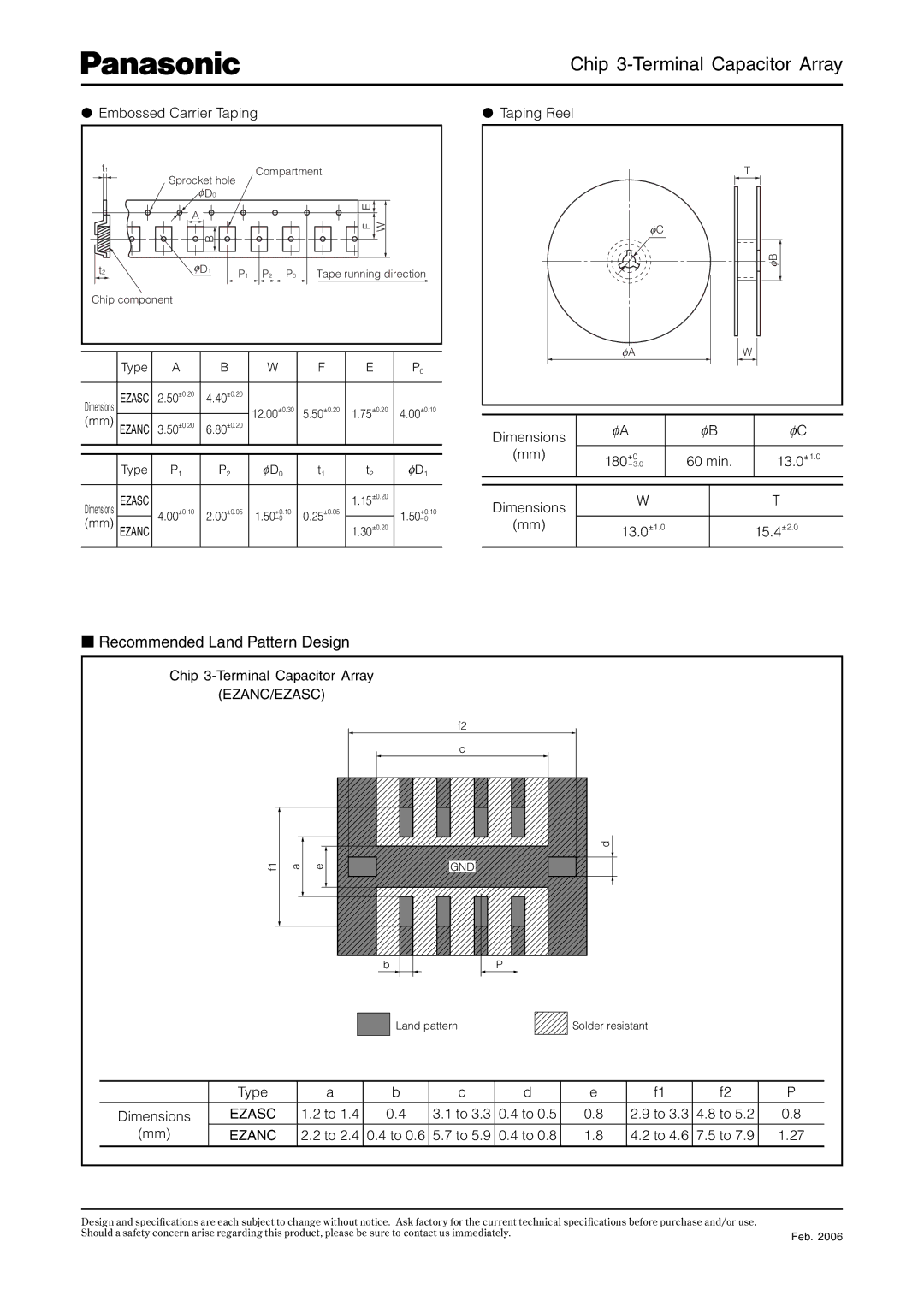
EZANC, EZASC specifications
Panasonic has long been a pioneer in the world of audio technology, and their latest offerings, the EZANC and EZASC, continue this legacy with remarkable advancements in sound quality and user experience. These cutting-edge devices are engineered to deliver an immersive audio journey that caters to the modern audiophile.The EZANC model is particularly notable for its superior noise cancellation technology. Panasonic has integrated advanced Adaptive Noise Cancelling (ANC) features, which dynamically adjust to environmental sounds. This ensures that users can enjoy their music or calls without distractions, whether they're in busy urban settings or quieter environments. The user can toggle between different ANC levels depending on the surrounding noise, providing versatile listening experiences.
On the other hand, the EZASC emphasizes superior sound quality with its high-resolution audio capabilities. It supports a wide range of audio formats, allowing users to enjoy music in its purest form. The device is equipped with a powerful DAC (Digital-to-Analog Converter) that minimizes distortion and ensures that every note is crystal clear. This makes the EZASC ideal for those who appreciate rich musical nuances, from thumping bass lines to shimmering highs.
Both models feature Bluetooth connectivity, ensuring seamless pairing with a variety of devices. The EZANC and EZASC utilize the latest Bluetooth codecs for enhanced audio transmission, making it possible to enjoy high-fidelity sound wirelessly. With extended battery life, users can enjoy uninterrupted playback for hours on end, further enhancing the convenience of these devices.
Additionally, ergonomic design is a hallmark of both models. They are crafted to provide comfort during extended use, with soft ear cushions and adjustable headbands. Whether you're working out, commuting, or simply chilling at home, these headphones ensure a snug fit without causing discomfort.
Both headphones come equipped with touch controls, allowing users to manage calls and playback effortlessly. Voice assistant compatibility makes it easy to access information hands-free, adding to the overall user-friendly experience.
In summary, Panasonic's EZANC and EZASC headphones embody a combination of innovative technology, superior sound quality, and user-centric design. These models are a testament to Panasonic's dedication to delivering exceptional audio experiences, making them an excellent choice for audio enthusiasts and everyday users alike.