4.0ATA interface
These drives use the
You can use a
4.1ATA interface signals and connector pins
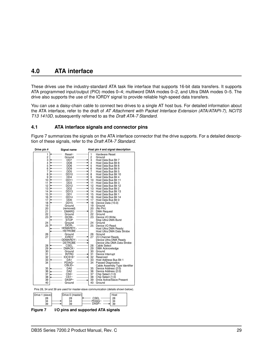
Figure 7 summarizes the signals on the ATA interface connector that the drive supports. For a detailed descrip- tion of these signals, refer to the Draft ATA-7 Standard.
Drive pin # |
|
| Signal name |
|
| Host pin # and signal description | ||||||||||||||||||||
1 |
|
|
|
|
|
|
|
|
|
| Reset– |
|
|
|
|
|
| 1 | Hardware Reset | |||||||
|
|
|
|
|
|
|
|
|
|
| ||||||||||||||||
2 |
|
|
|
|
|
|
|
|
|
| Ground | 2 | Ground | |||||||||||||
3 |
|
|
|
|
|
|
|
|
|
| DD7 |
|
| 3 | Host Data Bus Bit 7 | |||||||||||
|
|
|
|
|
|
|
| |||||||||||||||||||
4 |
|
|
|
|
|
|
|
|
|
| DD8 |
|
| 4 | Host Data Bus Bit 8 | |||||||||||
|
|
|
|
|
|
|
| |||||||||||||||||||
5 |
|
|
|
|
|
|
|
|
|
| DD6 |
|
| 5 | Host Data Bus Bit 6 | |||||||||||
|
|
|
|
|
|
|
| |||||||||||||||||||
6 |
|
|
|
|
|
|
|
|
|
| DD9 |
|
| 6 | Host Data Bus Bit 9 | |||||||||||
|
|
|
|
|
|
|
| |||||||||||||||||||
7 |
|
|
|
|
|
|
|
|
|
| DD5 |
|
| 7 | Host Data Bus Bit 5 | |||||||||||
|
|
|
|
|
|
|
| |||||||||||||||||||
8 |
|
|
|
|
|
|
|
|
|
| DD10 |
|
| 8 | Host Data Bus Bit 10 | |||||||||||
|
|
|
|
|
|
|
| |||||||||||||||||||
9 |
|
|
|
|
|
|
|
|
|
| DD4 |
|
| 9 | Host Data Bus Bit 4 | |||||||||||
|
|
|
|
|
|
|
| |||||||||||||||||||
10 |
|
|
|
|
|
|
|
|
|
| DD11 |
|
| 10 | Host Data Bus Bit 11 | |||||||||||
|
|
|
|
|
|
|
| |||||||||||||||||||
11 |
|
|
|
|
|
|
|
|
|
| DD3 |
|
| 11 | Host Data Bus Bit 3 | |||||||||||
|
|
|
|
|
|
|
| |||||||||||||||||||
12 |
|
|
|
|
|
|
|
|
|
| DD12 |
|
| 12 | Host Data Bus Bit 12 | |||||||||||
|
|
|
|
|
|
|
| |||||||||||||||||||
13 |
|
|
|
|
|
|
|
|
|
| DD2 |
|
| 13 | Host Data Bus Bit 2 | |||||||||||
|
|
|
|
|
|
|
| |||||||||||||||||||
14 |
|
|
|
|
|
|
|
|
|
| DD13 |
|
| 14 | Host Data Bus Bit 13 | |||||||||||
|
|
|
|
|
|
|
| |||||||||||||||||||
15 |
|
|
|
|
|
|
|
|
|
| DD1 |
|
| 15 | Host Data Bus Bit 1 | |||||||||||
|
|
|
|
|
|
|
| |||||||||||||||||||
16 |
|
|
|
|
|
|
|
|
|
| DD14 |
|
| 16 | Host Data Bus Bit 14 | |||||||||||
|
|
|
|
|
|
|
| |||||||||||||||||||
17 |
|
|
|
|
|
|
|
|
|
| DD0 |
|
| 17 | Host Data Bus Bit 0 | |||||||||||
|
|
|
|
|
|
|
| |||||||||||||||||||
18 |
|
|
|
|
|
|
|
|
|
| DD15 |
|
| 18 | Device Data (15:0) | |||||||||||
|
|
|
|
|
|
|
| |||||||||||||||||||
19 |
|
|
|
|
|
|
|
|
|
| Ground | 19 | Ground | |||||||||||||
20 |
|
|
|
|
|
|
|
|
|
| (removed) | 20 | (No Pin) | |||||||||||||
21 |
|
|
|
|
|
|
|
|
|
| DMARQ |
|
|
|
|
| 21 | DMA Request | ||||||||
|
|
|
|
|
|
|
|
|
|
| ||||||||||||||||
22 |
|
|
|
|
|
|
|
|
|
| Ground | 22 | Ground | |||||||||||||
23 |
|
|
|
|
|
|
|
|
|
| DIOW– |
|
|
|
|
|
|
| 23 | Device I/O Write: | ||||||
|
|
|
|
|
|
|
|
|
|
|
|
|
|
| ||||||||||||
|
|
|
|
|
|
|
|
|
|
| STOP |
|
|
|
|
|
|
|
|
|
| Stop Ultra DMA Burst | ||||
|
|
|
|
|
|
|
|
|
|
|
|
|
|
|
|
|
|
|
|
| ||||||
24 |
|
|
|
|
|
|
|
|
|
| Ground | 24 | Ground | |||||||||||||
25 |
|
|
|
|
|
|
|
|
|
| DIOR– |
|
|
|
|
|
| 25 | Device I/O Read: | |||||||
|
|
|
|
|
|
|
|
|
|
|
| |||||||||||||||
|
|
|
|
|
|
| HDMARDY– |
|
|
|
|
|
|
| Host Ultra DMA Ready: | |||||||||||
|
|
|
|
|
|
|
|
|
|
| HSTROBE |
|
|
|
|
|
|
|
|
| Host Ultra DMA Data Strobe | |||||
|
|
|
|
|
|
|
|
|
|
|
|
|
|
|
|
|
| |||||||||
26 |
|
|
|
|
|
|
|
|
|
| Ground | 26 | Ground | |||||||||||||
27 |
|
|
|
|
|
|
|
|
|
| IORDY |
|
|
|
|
| 27 | I/O Channel Ready | ||||||||
|
|
|
|
|
|
|
|
| ||||||||||||||||||
|
|
|
|
|
|
| DDMARDY– |
|
|
|
|
|
|
| Device Ultra DMA Ready | |||||||||||
|
|
|
|
|
|
|
|
|
|
|
|
|
| |||||||||||||
|
|
|
|
|
|
|
|
|
|
| DSTROBE |
|
|
|
|
|
|
|
| Device Ulta DMA Data Strobe | ||||||
|
|
|
|
|
|
|
|
|
|
|
|
|
|
|
|
| ||||||||||
28 |
|
|
|
|
|
|
|
|
|
| CSEL |
|
|
|
|
|
| 28 | Cable Select | |||||||
|
|
|
|
|
|
|
|
|
|
| ||||||||||||||||
29 |
|
|
|
|
|
|
|
|
|
| DMACK– |
|
|
|
|
|
|
| 29 | DMA Acknowledge | ||||||
|
|
|
|
|
|
|
|
|
|
|
| |||||||||||||||
30 |
|
|
|
|
|
|
|
|
|
| Ground | 30 | Ground | |||||||||||||
31INTRQ ![]() 31 Device Interrupt
31 Device Interrupt
32IOCS16– ![]() 32 Reserved
32 Reserved
33 |
|
|
| DA1 |
|
| 33 | Host Address Bus Bit 1 | |
|
|
| |||||||
34 |
|
|
| PDIAG– |
|
| 34 | Passed Diagnostics | |
|
|
|
| CBLID– |
|
|
| Cable Assembly Type Identifier | |
35 |
|
|
| DA0 |
|
| 35 | Device Address (2:0) | |
|
|
|
|
| |||||
36 |
|
|
| DA2 |
|
| 36 | Device Address (2:0) | |
37 |
|
|
| CS0– |
|
|
| 37 | Chip Select (1:0) |
38 |
|
|
| CS1– |
|
|
| 38 | Chip Select (1:0) |
39 |
|
|
| DASP– |
| 39 | Drive Active/Slave Present | ||
|
|
|
| ||||||
40 |
|
|
| Ground | 40 | Ground | |||
Pins 28, 34 and 39 are used for
Drive 1 (slave)
28
34
39
Figure 7
Drive 0 (master) |
|
|
|
|
| Host |
28 |
| CSEL |
| 28 | ||
|
| |||||
34 |
| PDIAG– |
|
| 34 | |
|
|
| ||||
39 |
| DASP– |
|
| 39 | |
|
| |||||
I/O pins and supported ATA signals
DB35 Series 7200.2 Product Manual, Rev. C | 29 |