IV? 7ce
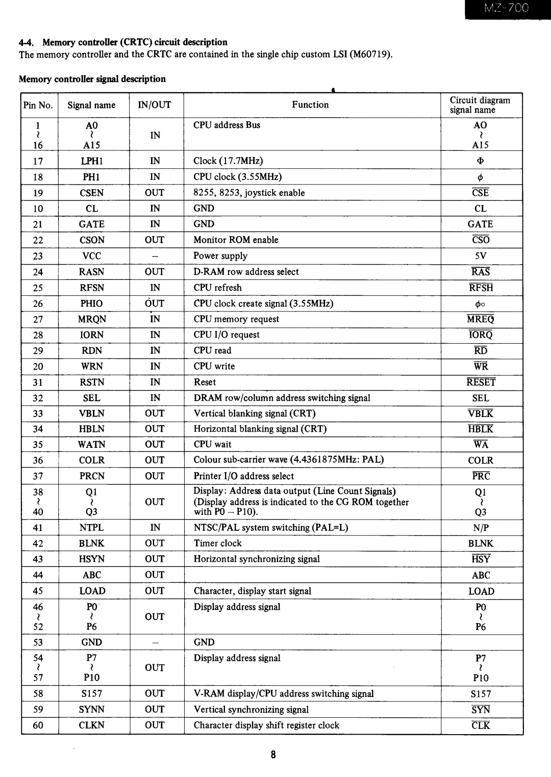
The memory controller and the CRTC are contained in the single chip custom LSI (M60719).
Memory controller signal description
|
|
|
| & |
| ||
| Pin No. | Signal name | IN/OUT |
| Function | Circuit diagram | |
|
| signal name | |||||
|
|
|
|
|
| ||
|
|
|
|
|
|
| |
1 | AO |
| CPU address Bus | AO | |||
| l | l | IN |
|
| l | |
16 | A15 |
|
|
| A15 | ||
17 | LPH1 | IN | Clock (17.7MHz) | <I> | |||
|
|
|
|
|
|
| |
18 | PHI | IN | CPU clock (3.55MHz) | cp | |||
|
|
|
|
|
|
| |
19 | CSEN | OUT | 8255, 8253, joystick enable | CSE | |||
|
|
|
|
|
|
| |
10 | CL | IN | GND | CL | |||
|
|
|
|
|
|
| |
21 | GATE | IN | GND | GATE | |||
|
|
|
|
|
|
| |
22 | CSON | OUT | Monitor ROM enable | CSO | |||
|
|
|
|
|
|
| |
23 | VCC | - | Power supply | 5V | |||
|
|
|
|
|
|
| |
24 | RASN | OUT | RAS | ||||
|
|
|
|
|
|
| |
25 | RFSN | IN | CPU refresh | RFSH | |||
|
|
|
|
|
|
| |
26 | PHIO | OUT | CPU clock create signal (3.55MHz) | cpo | |||
|
|
|
|
|
|
| |
27 | MRQN | IN | CPU memory request | MREQ | |||
|
|
|
|
|
|
| |
28 | 10RN | IN | CPU I/O request | IORQ | |||
|
|
|
|
|
|
| |
29 | RDN | IN | CPU read | RD | |||
|
|
|
|
|
|
| |
20 | WRN | IN | CPU write | WR | |||
|
|
|
|
|
|
| |
31 | RSTN | IN | Reset | RESET | |||
|
|
|
|
|
|
| |
32 | SEL | IN | DRAM row/column address switching signal | SEL | |||
|
|
|
|
|
|
| |
33 | VBLN | OUT | Vertical blanking signal (CRT) | VBLK | |||
|
|
|
|
|
|
| |
34 | HBLN | OUT | Horizontal blanking signal (CRT) | HBLK | |||
|
|
|
|
|
|
| |
35 | WATN | OUT | CPU wait | WA | |||
|
|
|
|
|
|
| |
36 | COLR | OUT | Colour | COLR | |||
|
|
|
|
|
|
| |
37 | PRCN | OUT | Printer I/O address select | PRC | |||
|
|
|
|
|
|
| |
38 | Q1 |
| Display: Address data output (Line Count Signals) | Ql | |||
| l | l | OUT | (Display address is indicated to the CG ROM together | l | ||
| 40 | Q3 |
| with PO - PlO). | Q3 | ||
|
| ||||||
|
|
|
|
|
|
| |
| 41 | NTPL | IN | NTSC/PAL system switching (PAL=L) | N/P | ||
|
|
|
|
|
|
| |
| 42 | BLNK | OUT | Timer clock | BLNK | ||
|
|
|
|
|
|
| |
| 43 | HSYN | OUT | Horizontal synchronizing signal | HSY | ||
|
|
|
|
|
|
| |
| 44 | ABC | OUT |
|
| ABC | |
|
|
|
|
|
| ||
| 45 | LOAD | OUT | Character, display start signal | LOAD | ||
|
|
|
|
|
| ||
| 46 | PO | OUT | Display address signal | PO | ||
| l | ~ |
|
| l | ||
| 52 | P6 |
|
|
| P6 | |
|
|
|
|
|
| ||
| 53 | GND | - | GND |
| ||
|
|
|
|
|
| ||
| 54 | P7 |
| Display address signal | P7 | ||
| l | l | OUT |
|
| l | |
| 57 | PlO |
|
|
| PlO | |
|
|
|
|
|
| ||
| 58 | S157 | OUT | S157 | |||
|
|
|
|
|
| ||
| 59 | SYNN | OUT | Vertical synchronizing signal | SYN | ||
|
|
|
|
|
| ||
| 60 | CLKN | OUT | Character display shift register clock | CLK | ||
|
|
|
|
|
|
| |
8