
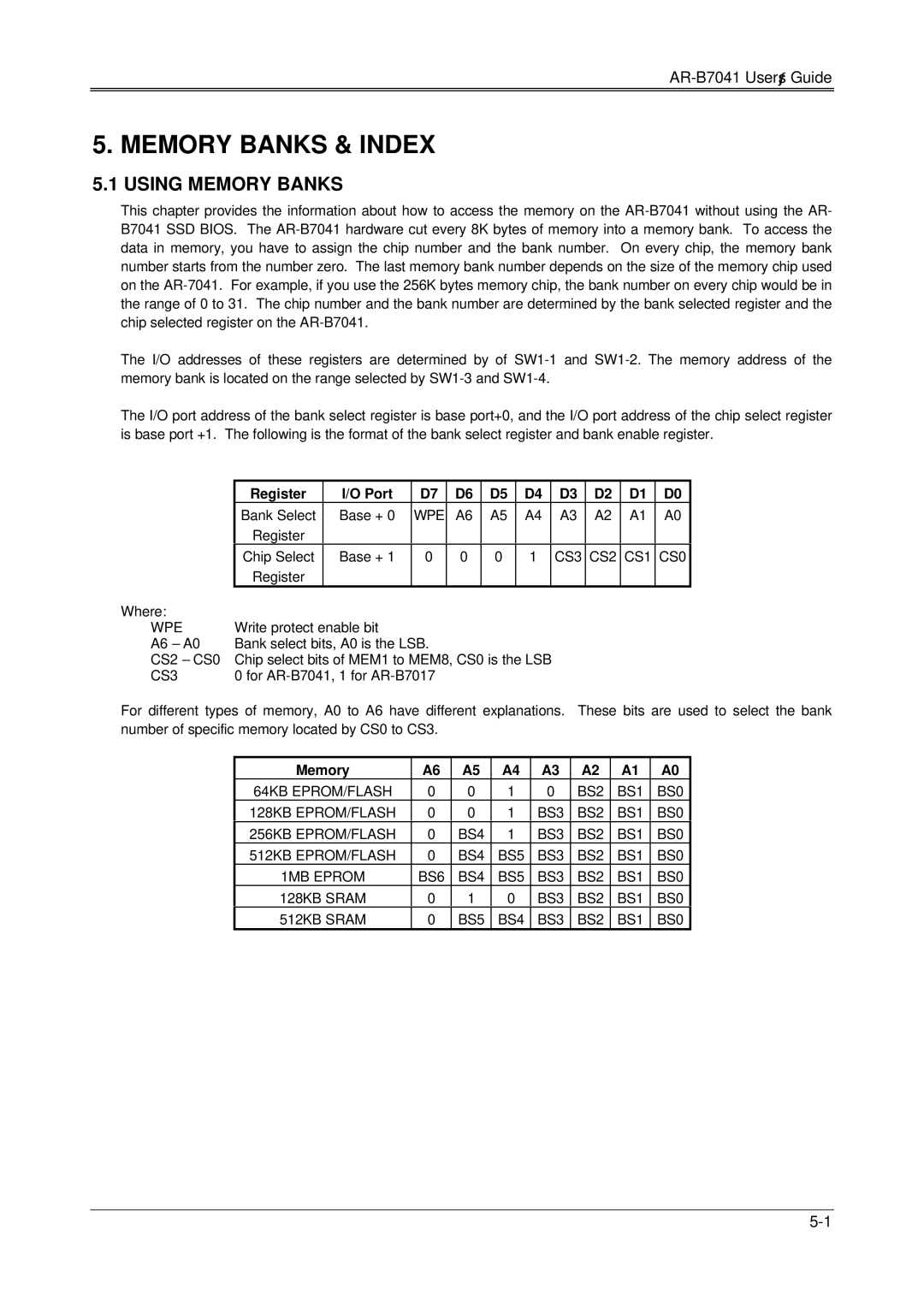
AR-B7041 specifications
The Solid State Logic AR-B7041 is a groundbreaking audio production console that epitomizes the integration of advanced technology with traditional analog warmth. Designed for both studio and live applications, the AR-B7041 stands as a testament to Solid State Logic’s commitment to quality and innovation in audio engineering.At the heart of the AR-B7041 is its exceptional analog signal path, which ensures that every audio source is captured and processed with remarkable fidelity. The console features high-performance mic preamps, known for their low noise floor and exceptional headroom. This allows engineers to achieve clarity and detail, making it suitable for a wide range of applications, from recording studios to live sound reinforcement.
One of the standout features of the AR-B7041 is its extensive routing capabilities. With multiple bus configurations and flexible patching options, users can customize their workflow to fit their unique production styles. This versatility is further enhanced by the integrated digital connectivity, allowing seamless integration with digital audio workstations (DAWs) and other digital equipment. The dual-functionality of analog and digital processes makes it a perfect fit for modern hybrid studios.
The interface of the AR-B7041 is designed with user-friendliness in mind, offering an intuitive layout that allows for quick adjustments and easy navigation. The console includes an array of user-definable buttons and faders, providing engineers the ability to create personalized setups that streamline their workflow. Moreover, the built-in monitoring capabilities ensure accurate audio assessment, critical for achieving the best sonic results.
Incorporating advanced technologies like dynamic EQ and multi-effects processing, the AR-B7041 caters to the evolving demands of audio engineering. These features not only enhance sound shaping but also save valuable studio time by allowing engineers to achieve polished sounds in real time.
Durability and reliability are hallmarks of the Solid State Logic brand, and the AR-B7041 is no exception. Constructed with high-quality materials, it is designed to withstand the rigors of daily studio or live performance usage, ensuring longevity without compromising performance.
In summary, the Solid State Logic AR-B7041 is a versatile and sophisticated audio production console that combines traditional analog characteristics with modern technological advancements. Its impressive features, robust routing capabilities, and user-friendly design make it an essential tool for audio professionals seeking both flexibility and excellence in sound quality.