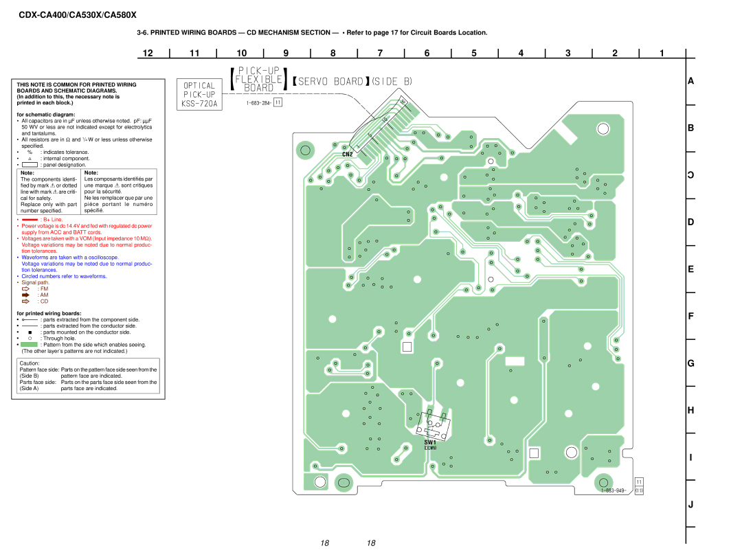
CDX-CA580X, CDX-CA400, CDX-CA530X specifications
The Sony CDX-CA530X, CDX-CA400, and CDX-CA580X are notable entries in the realm of car audio systems, offering a range of features that cater to both functionality and connectivity, making them excellent companions for any driver who values high-quality sound.The Sony CDX-CA530X is distinguished by its sleek design and user-friendly interface. It supports CD playback, AM/FM radio, and comes equipped with a front auxiliary input for easy connection of portable devices. This model is designed with a built-in dynamic bass boost, which enriches the low-frequency response, delivering a more immersive listening experience. Additionally, the CDX-CA530X supports various audio formats, allowing users to enjoy their favorite music in different formats easily. Its LCD display provides clear visibility of track information, making it easy for users to navigate through their playlists.
Next in line is the CDX-CA400, which offers a budget-friendly yet feature-rich option for car audio enthusiasts. This model focuses on simplicity and reliability without compromising sound quality. It also facilitates AM/FM radio and CD playback, enhanced with an easy-to-read display. The CDX-CA400 comes equipped with preamp outputs, enabling users to expand their audio system by adding external amplifiers. The model excels in user accessibility with its straightforward controls and responsive buttons, ensuring users can quickly switch tracks or adjust volume while driving.
The Sony CDX-CA580X takes sound quality a step further with advanced features that appeal to audiophiles. It incorporates CD-R/RW playback, enhancing the versatility of music sources. With its built-in equalizer, the CDX-CA580X allows users to customize their audio settings to suit their preferences, optimizing sound quality based on genre or personal taste. The unit also supports front-panel USB connectivity, enabling seamless integration with USB drives and smart devices. This model boasts a robust amplifier, delivering powerful audio performance that stands out even at high volumes.
All three models reflect Sony’s commitment to innovation and quality in the automotive audio landscape. They emphasize practical technologies such as seamless integration with various playback mediums, intuitive interfaces, and robust sound enhancement capabilities. Whether you choose the CDX-CA530X, CDX-CA400, or CDX-CA580X, you can expect a listening experience that enriches your driving journey, blending convenience with exceptional audio performance tailored to meet a variety of needs.

