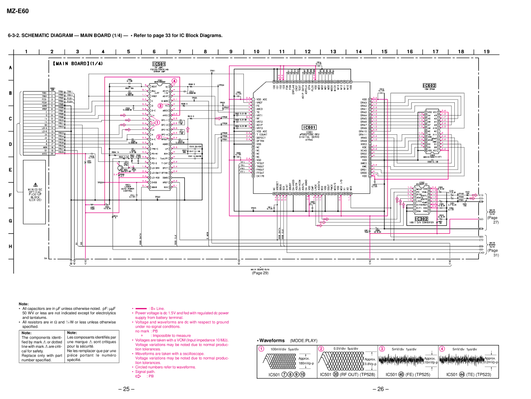
MZ-E90 specifications
The Sony MZ-E90 is a notable portable mini-disc player, emblematic of early 2000s technology that revolutionized how music was consumed. Launched during a time when CDs and cassette tapes were dominant, the MZ-E90 provided a compact solution for digital audio playback, embodying Sony's commitment to audio quality and portability.One of the standout features of the MZ-E90 is its ability to record audio in real-time. Users can easily create their own mini-discs by recording tracks directly from a CD, vinyl, or even from the radio. This flexibility allowed music enthusiasts to curate personalized playlists on a single medium, which was a significant advantage over traditional physical formats.
The player utilizes Sony's ATRAC (Adaptive TRAnsform Acoustic Coding) compression technology, which enables high-quality sound reproduction in a space-efficient manner. The MZ-E90 supports MDLP (MiniDisc Long Play) mode, allowing users to store multiple albums on a single disc. This capability enhanced its appeal, especially for those with extensive music collections.
In terms of design, the MZ-E90 is compact and lightweight, making it easy to transport. The player features a user-friendly interface, equipped with a backlit LCD display that shows track information and playback status. The controls are intuitive, allowing users to navigate through their music selections effortlessly.
Battery life is another crucial aspect of the MZ-E90, offering long playback hours thanks to its efficient power management. This aspect made it a preferable choice for those on the go, as it ensured that users could enjoy their music for extended periods without frequent recharging.
Moreover, the MZ-E90 includes a headphone jack for private listening and features an integrated bass boost function that augments low-frequency sounds, enhancing the listening experience for those who enjoy richer audio. The use of high-quality components further ensures that the sound reproduction does justice to the original recordings.
While the Sony MZ-E90 may not have the mainstream recognition of today’s streaming platforms, it played a pivotal role in advancing portable digital music technology. Its combination of recording capabilities, sound quality, and portability made it a cherished device for audiophiles and casual listeners alike during its production run. The legacy of such devices remains evident in the evolution of portable music, paving the way for modern digital audio players and streaming services.

