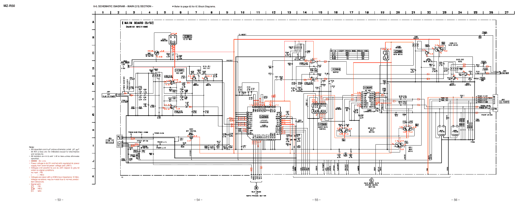
MZ-R50 specifications
The Sony MZ-R50, launched in the late 1990s, is a notable model in the MiniDisc player genre, which revolutionized how consumers listened to music. Part of Sony's first generation of MiniDisc recorders, the MZ-R50 quickly gained popularity for its sleek design and innovative features.One of the standout features of the MZ-R50 is its compact size and lightweight construction. It weighs just 160 grams, making it one of the most portable audio devices of its time. This portability paired with a stylish aesthetic allowed users to carry their music with ease, appealing to young, active lifestyles.
The MZ-R50 utilizes MiniDisc technology, which employs a small, flat disc encased in a protective shell. This format offers superior sound quality compared to cassette tapes, allowing for digital recording and playback. Users can record audio directly onto the disc in real-time or transfer music from CDs with ease. The player supports several recording modes, including LP2 and LP4, which allow users to maximize recording time without sacrificing quality.
Another significant feature of the MZ-R50 is its impressive battery life. It can run for up to 10 hours on a single charge, enabling long listening sessions without frequent recharging. The device also includes a digital pitch control, allowing users to change the tempo of tracks without affecting the pitch, which is especially useful for musicians and DJs.
Moreover, the MZ-R50 incorporates Sony's ATRAC (Adaptive Transform Acoustic Coding) compression technology. This advanced algorithm was designed to reduce the file size of audio while maintaining high sound fidelity, ensuring that music stored on MiniDiscs sounded close to the original recording. The player is compatible with both standard and long-play MiniDiscs, providing flexibility for users who want to store more music on a single disc.
In terms of connectivity, the MZ-R50 features an optical input for high-quality digital recording from other devices, along with a headphone output and a line out option for connecting to external speakers or audio systems. Its user-friendly interface allows for easy navigation through tracks and playlists, making it accessible for users of all ages.
Overall, the Sony MZ-R50 remains a beloved piece of audio technology, reflecting a unique combination of portability, sound quality, and user-friendly features, establishing its place in the history of personal music players. Its legacy continues to inspire later generations of audio enthusiasts.

