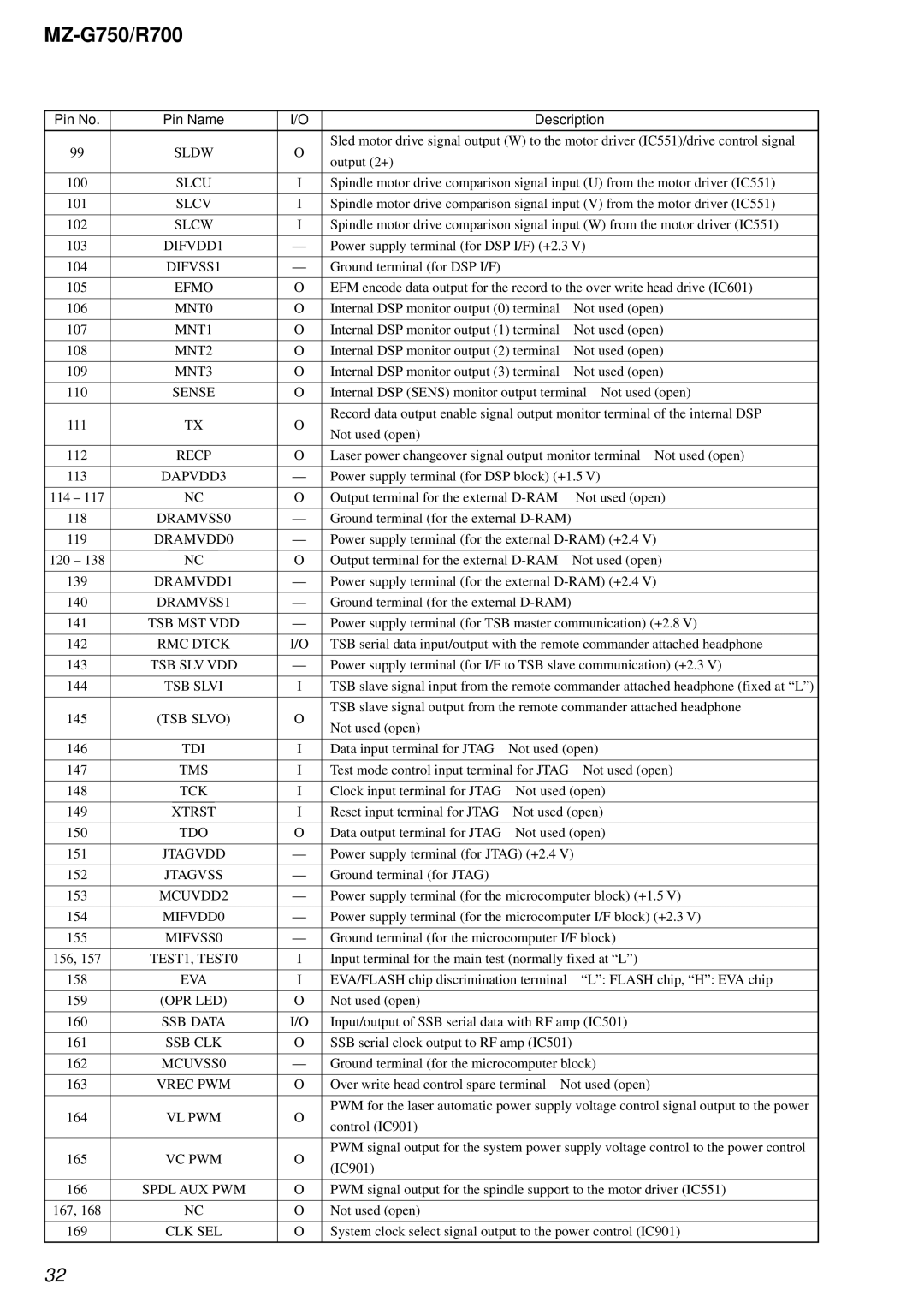
MZ-R700 specifications
The Sony MZ-R700 is a compact digital minidisc recorder that has made a significant mark in the portable audio landscape since its introduction. Known for its outstanding sound quality and portable design, it appeals to audiophiles and casual listeners alike. The MZ-R700 is lauded for its ability to record and playback high-quality audio, making it a go-to device for musicians, DJs, and anyone who values sound fidelity.One of the main features of the MZ-R700 is its ability to record music in various formats. It supports the ATRAC (Adaptive Transform Acoustic Coding) compression format, which allows users to store more audio data on a minidisc while maintaining remarkable sound clarity. This technology ensures that even with compression, the audio remains rich and engaging.
The MZ-R700 comes equipped with a digital recording feature, enabling users to transfer tracks directly from CDs or other digital sources without sacrificing quality. It is compatible with a wide range of digital audio formats, allowing for flexibility in recording options. Additionally, the device offers various recording modes, giving users the choice between standard quality and long-play modes, depending on their needs.
Portability is a key characteristic of the MZ-R700. Weighing just a few ounces and featuring a sleek, ergonomic design, it fits comfortably in the hand and can easily be carried in a pocket or bag. Its user-friendly interface includes an LCD screen that displays track information, making it easy for users to navigate through their music library.
Another notable feature is its battery efficiency. The MZ-R700 is powered by a rechargeable lithium-ion battery, providing extended playback time. Users can enjoy hours of continuous music playback, making it perfect for long journeys or outdoor activities.
The popular mic input allows for live recordings, a feature that musicians and podcasters find particularly beneficial. Moreover, the unit supports various input options, including a line-in and a 3.5mm microphone jack, ensuring versatility for different recording needs.
In summary, the Sony MZ-R700 is a robust and feature-rich digital minidisc recorder that combines portability, superior sound quality, and user-friendly design. With advanced recording technologies and efficient battery life, it caters to a variety of audio enthusiasts, making it a remarkable choice for portable sound recording and playback.
