
PCGA-DSM5, PCGA-DSD5 specifications
The Sony PCGA-DSD5 and PCGA-DSM5 are notable accessories designed for Sony laptops, primarily enhancing the portability and functionality of these devices. These products cater to users seeking efficient solutions for data storage, expansion, and connectivity.The PCGA-DSD5, also known as the Sony SuperDisk Drive, is designed to read and write a variety of disc formats, including DVD and CD media. It stands out due to its compatibility with high-capacity floppy disks, ensuring users can access legacy data while also incorporating modern storage solutions. With a lightweight and compact design, the PCGA-DSD5 is perfect for users on the go, making it easy to carry alongside the laptop.
Another significant feature of the PCGA-DSD5 is its plug-and-play functionality. This allows for seamless integration with compatible Sony laptops, eliminating the need for complex installation procedures. Users can quickly start using the drive without intricate setups, which is particularly beneficial for those who require immediate access to data.
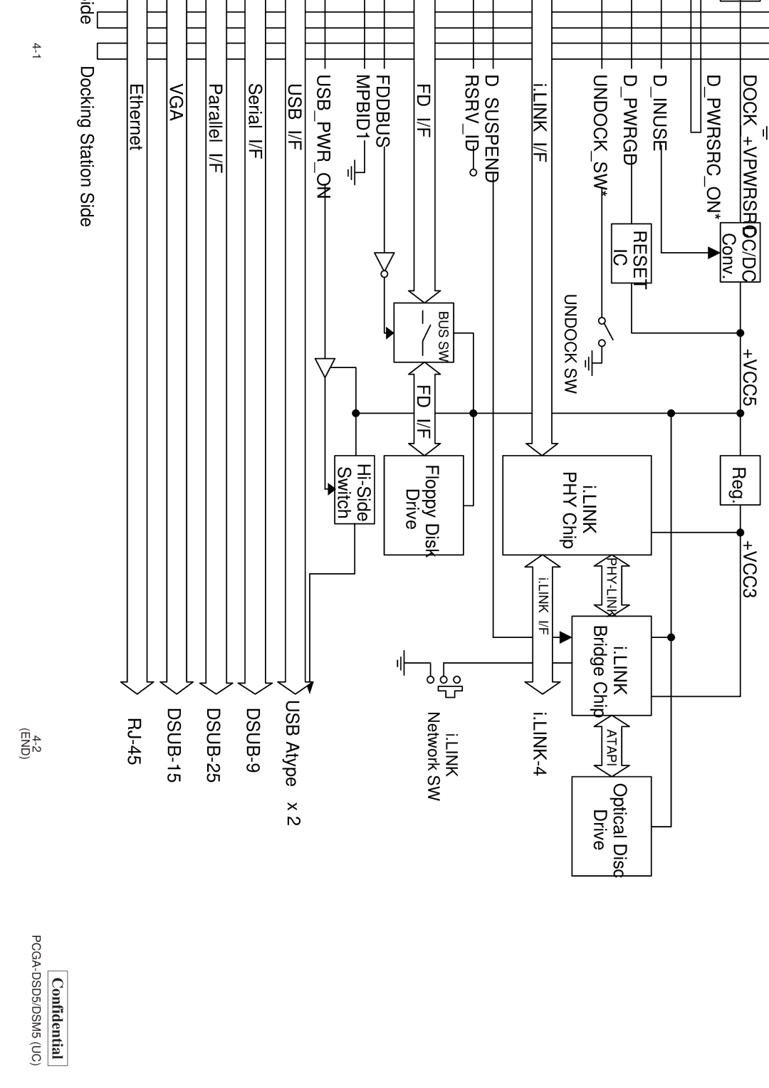
On the other hand, the PCGA-DSM5 serves as a docking station, providing extensive connectivity options that enhance the productivity of users by turning the laptop into a workstation. This docking station features multiple ports, including USB, Ethernet, and audio jacks, which allow users to connect various peripherals easily. This connectivity is vital for professionals who require multiple devices, such as printers, external hard drives, and monitors.
The PCGA-DSM5 also helps organize desktop spaces, allowing users to manage cables and connections neatly. Its design typically supports multiple displays, enabling users to expand their visual workspace significantly. This feature is especially useful for tasks that require multitasking, such as data analysis or content creation.
Both the PCGA-DSD5 and PCGA-DSM5 are built with durability in mind, reflecting Sony's commitment to quality. They are designed to withstand daily use and transport, ensuring longevity in performance. Additionally, they incorporate cutting-edge technologies to ensure fast data transfer and reliable connections, underlining their relevance in today's digital environment.
In summary, the Sony PCGA-DSD5 and PCGA-DSM5 are instrumental in enhancing the functionality and versatility of Sony laptops. With their robust features, seamless connectivity, and portability, they cater to both casual users and professionals, making them essential tools for enhancing productivity and accessing data efficiently.