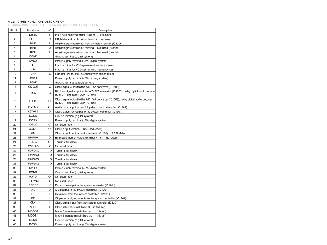
STR-DE845 specifications
The Sony STR-DE845 is a vintage yet impressive 5.1-channel surround sound receiver that has captivated audio enthusiasts since its release. As part of Sony's esteemed line of home audio equipment, this model exemplifies a combination of classic design, robust build quality, and advanced features that enhance the listening experience.One of the standout features of the STR-DE845 is its power output, capable of delivering 100 watts per channel at 8 ohms. This ample power ensures that your audio experience remains vibrant and dynamic, whether you’re enjoying music or watching movies. The receiver supports a range of speaker configurations, making it versatile enough to accommodate various home theater setups.
Another key characteristic of the STR-DE845 is its compatibility with Dolby Pro Logic and DTS surround sound formats. These technologies bring a cinematic experience into the home, allowing sound to envelop listeners from all directions. The receiver's ability to decode these formats enhances the clarity and immersion of soundtracks, providing an impressive auditory experience.
The STR-DE845 boasts a wide array of connectivity options, including multiple analog and digital inputs, which allow you to connect various audio sources such as CD players, VCRs, and gaming consoles. The inclusion of an AM/FM tuner also opens up the possibility for listening to local radio stations. For convenience, the receiver includes a remote control, enabling users to adjust settings and change inputs from a distance.
In terms of audio processing, the STR-DE845 features Advanced Digital Sound Field Processing (DSFP), which allows users to customize their listening experience based on room acoustics and personal preferences. This technology helps replicate the ambiance of live music venues and movie theaters, delivering an optimized sound experience regardless of the room's characteristics.
The design of the STR-DE845 is another highlight. With a sleek black finish and intuitive layout, this receiver fits seamlessly into any home entertainment setup. The front panel features a clear display, and the user-friendly interface makes navigating settings and configurations straightforward.
Moreover, the receiver's durability is noteworthy. Built with quality components, the STR-DE845 is designed to withstand the test of time, making it a dependable option for audiophiles and casual listeners alike.
In conclusion, the Sony STR-DE845 is a feature-packed surround sound receiver that combines quality, functionality, and a user-friendly experience. With its powerful output, advanced surround sound technologies, and versatility in connectivity, it remains a respectable choice for those looking to elevate their audio and home theater systems.
