XR-M510
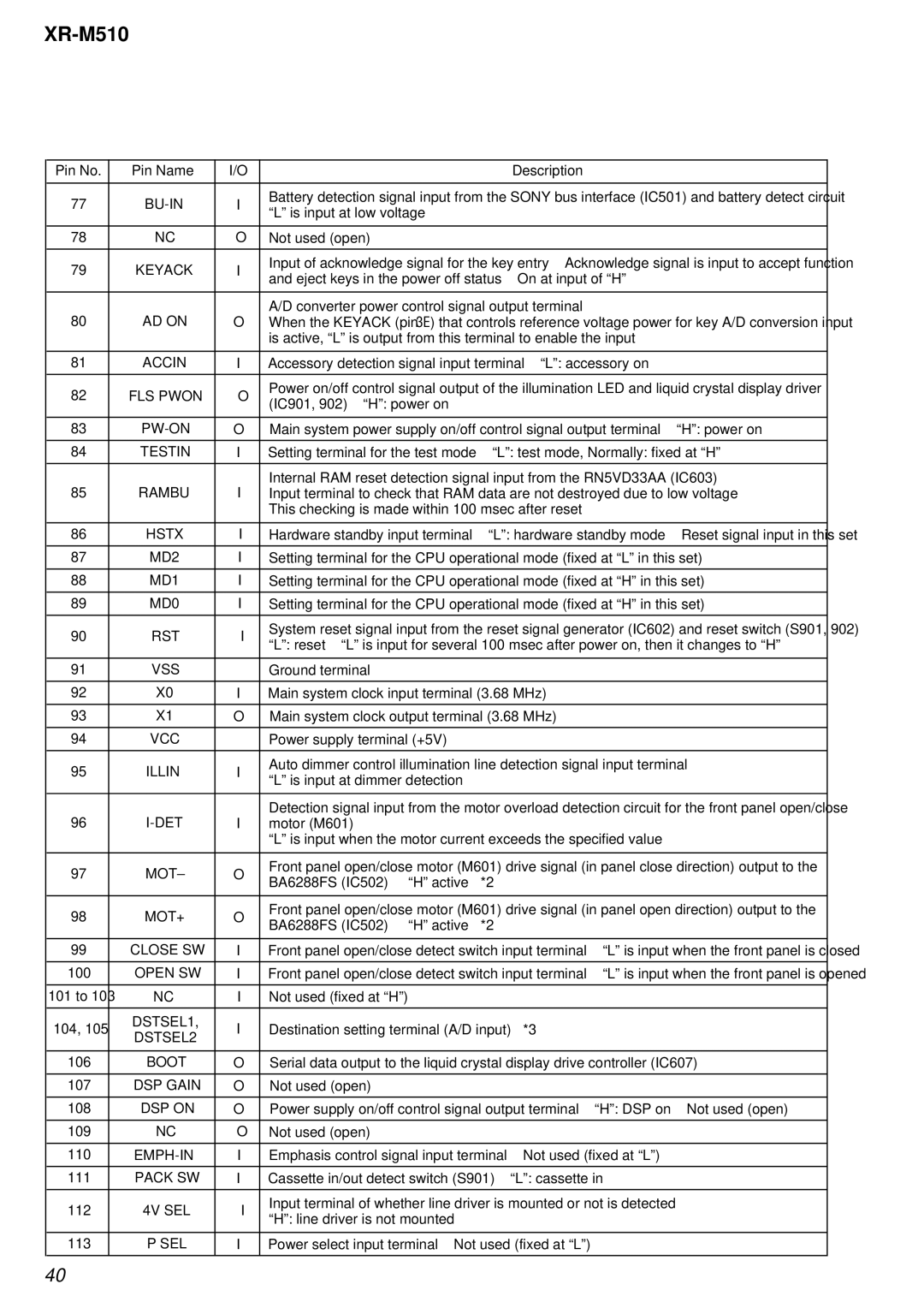
Pin No. | Pin Name | I/O |
|
|
|
| Description |
| |||
|
|
|
|
|
| ||||||
77 |
|
| I | Battery detection signal input from the SONY bus interface (IC501) and battery detect circuit | |||||||
| “L” is input at low voltage |
|
|
|
|
| |||||
|
|
|
|
|
|
|
|
|
| ||
|
|
|
|
|
|
|
|
|
|
|
|
78 |
| NC | O | Not used (open) |
|
|
|
|
|
| |
|
|
|
|
|
| ||||||
79 |
| KEYACK | I | Input of acknowledge signal for the key entry Acknowledge signal is input to accept function | |||||||
| and eject keys in the power off status | On at input of “H” |
| ||||||||
|
|
|
|
|
| ||||||
|
|
|
|
|
|
|
| ||||
80 |
| AD ON |
| A/D converter power control signal output terminal |
|
| |||||
| O | When the KEYACK (pin ul) that controls reference voltage power for key A/D conversion input | |||||||||
|
|
|
|
| is active, “L” is output from this terminal to enable the input |
| |||||
|
|
|
|
|
|
| |||||
81 |
| ACCIN | I | Accessory detection signal input terminal “L”: accessory on |
| ||||||
|
|
|
|
|
| ||||||
82 | FLS PWON | O | Power on/off control signal output of the illumination LED and liquid crystal display driver | ||||||||
(IC901, 902) “H”: power on |
|
|
|
|
| ||||||
|
|
|
|
|
|
|
|
|
| ||
|
|
|
|
|
| ||||||
83 |
| O | Main system power supply on/off control signal output terminal | “H”: power on | |||||||
|
|
|
|
|
| ||||||
84 |
| TESTIN | I | Setting terminal for the test mode | “L”: test mode, Normally: fixed at “H” | ||||||
|
|
|
|
|
| ||||||
85 |
| RAMBU | I | Internal RAM reset detection signal input from the RN5VD33AA (IC603) | |||||||
| Input terminal to check that RAM data are not destroyed due to low voltage | ||||||||||
|
|
|
|
| This checking is made within 100 msec after reset |
|
| ||||
|
|
|
|
|
|
| |||||
86 |
| HSTX | I | Hardware standby input terminal | “L”: hardware standby mode | Reset signal input in this set | |||||
|
|
|
|
| |||||||
87 |
| MD2 | I | Setting terminal for the CPU operational mode (fixed at “L” in this set) | |||||||
|
|
|
|
| |||||||
88 |
| MD1 | I | Setting terminal for the CPU operational mode (fixed at “H” in this set) | |||||||
|
|
|
|
| |||||||
89 |
| MD0 | I | Setting terminal for the CPU operational mode (fixed at “H” in this set) | |||||||
|
|
|
|
|
| ||||||
90 |
| RST | I | System reset signal input from the reset signal generator (IC602) and reset switch (S901, 902) | |||||||
| “L”: reset “L” is input for several 100 msec after power on, then it changes to “H” | ||||||||||
|
|
|
|
| |||||||
|
|
|
|
|
|
|
|
|
|
| |
91 |
| VSS | — | Ground terminal |
|
|
|
|
|
| |
|
|
|
|
|
|
| |||||
92 |
| X0 | I | Main system clock input terminal (3.68 MHz) |
|
| |||||
|
|
|
|
|
|
| |||||
93 |
| X1 | O | Main system clock output terminal (3.68 MHz) |
|
| |||||
|
|
|
|
|
|
|
|
|
| ||
94 |
| VCC | — | Power supply terminal (+5V) |
|
|
|
|
| ||
|
|
|
|
|
| ||||||
95 |
| ILLIN | I | Auto dimmer control illumination line detection signal input terminal | |||||||
| “L” is input at dimmer detection |
|
|
|
|
| |||||
|
|
|
|
|
|
|
|
|
| ||
|
|
|
|
|
| ||||||
96 |
|
|
| Detection signal input from the motor overload detection circuit for the front panel open/close | |||||||
| I | motor (M601) |
|
|
|
|
|
| |||
|
|
|
|
| “L” is input when the motor current exceeds the specified value |
| |||||
|
|
|
|
|
| ||||||
97 |
| MOT– | O | Front panel open/close motor (M601) drive signal (in panel close direction) output to the | |||||||
| BA6288FS (IC502) | “H” active | *2 |
|
|
|
| ||||
|
|
|
|
|
|
|
|
| |||
|
|
|
|
|
| ||||||
98 |
| MOT+ | O | Front panel open/close motor (M601) drive signal (in panel open direction) output to the | |||||||
| BA6288FS (IC502) | “H” active | *2 |
|
|
|
| ||||
|
|
|
|
|
|
|
|
| |||
|
|
|
|
| |||||||
99 | CLOSE SW | I | Front panel open/close detect switch input terminal | “L” is input when the front panel is closed | |||||||
|
|
|
|
| |||||||
100 | OPEN SW | I | Front panel open/close detect switch input terminal | “L” is input when the front panel is opened | |||||||
|
|
|
|
|
|
|
|
|
|
| |
101 to 103 |
| NC | I | Not used (fixed at “H”) |
|
|
|
|
|
| |
|
|
|
|
|
|
|
|
|
| ||
104, 105 | DSTSEL1, | I | Destination setting terminal (A/D input) | *3 |
|
| |||||
| DSTSEL2 |
|
| ||||||||
|
|
|
|
|
|
|
|
|
| ||
|
|
|
|
|
| ||||||
106 |
| BOOT | O | Serial data output to the liquid crystal display drive controller (IC607) | |||||||
|
|
|
|
|
|
|
|
|
| ||
107 | DSP GAIN | O | Not used (open) |
|
|
|
|
|
| ||
|
|
|
|
|
|
| |||||
108 |
| DSP ON | O | Power supply on/off control signal output terminal | “H”: DSP on | Not used (open) | |||||
|
|
|
|
|
|
|
|
|
|
| |
109 |
| NC | O | Not used (open) |
|
|
|
|
|
| |
|
|
|
|
|
|
| |||||
110 |
| I | Emphasis control signal input terminal | Not used (fixed at “L”) |
| ||||||
|
|
|
|
|
|
| |||||
111 | PACK SW | I | Cassette in/out detect switch (S901) | “L”: cassette in |
|
| |||||
|
|
|
|
|
| ||||||
112 |
| 4V SEL | I | Input terminal of whether line driver is mounted or not is detected | |||||||
| “H”: line driver is not mounted |
|
|
|
|
| |||||
|
|
|
|
|
|
|
|
|
| ||
|
|
|
|
|
|
| |||||
113 |
| P SEL | I | Power select input terminal Not used (fixed at “L”) |
|
| |||||
|
|
|
|
|
|
|
|
|
|
|
|
40