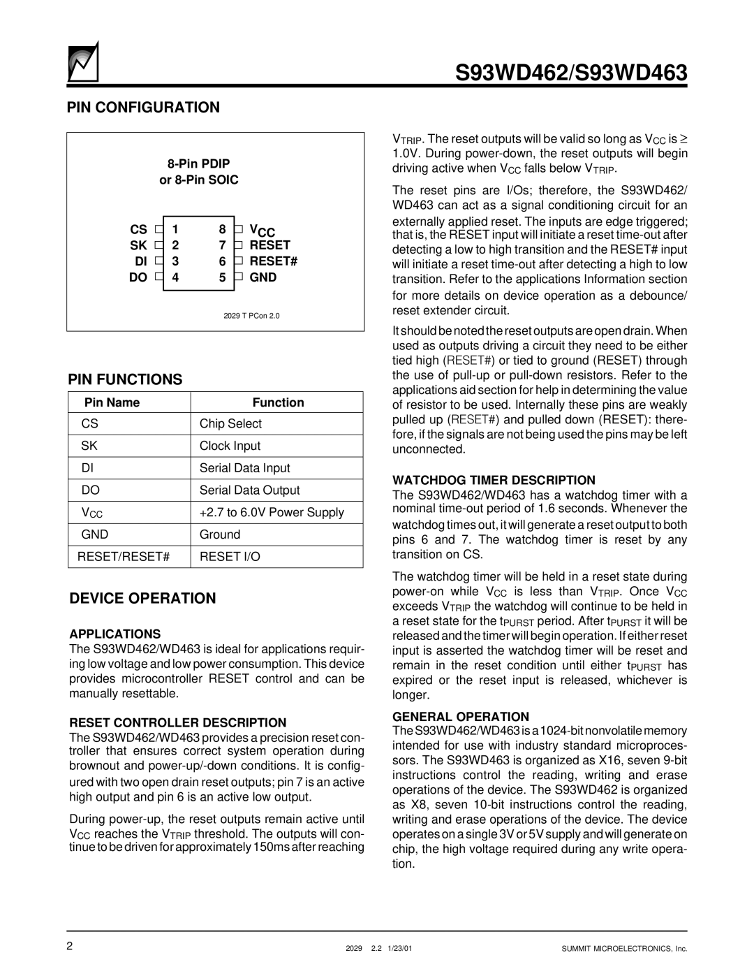
S93WD462, S93WD463 specifications
The Summit S93WD462 and S93WD463 stand out as prime examples of modern technology in compact refrigeration solutions. Designed for both residential and commercial use, these models offer several features that cater to varied needs.One of the primary characteristics of the S93WD462 and S93WD463 is their sleek, space-efficient design, ideal for smaller kitchens, apartments, or offices. The footprint of these models allows for installation in tight spaces while still providing ample capacity for storage. Both units are available in finishes that blend seamlessly with contemporary decor, enhancing the overall aesthetics of any environment.
When it comes to performance, these refrigerators are equipped with advanced cooling technologies. The frost-free cooling system ensures that users never have to deal with ice build-up, making maintenance effortless. This system also maintains a consistent interior temperature, which is crucial for preserving food quality and freshness over time.
Energy efficiency is another hallmark of the Summit S93WD series. These refrigerators are designed to consume less energy than standard models, thanks to features such as high-efficiency compressors and insulation technology. This not only reduces electricity bills but also contributes positively to environmental conservation.
Organizational features are thoughtfully integrated into the design of both models. Adjustable shelves provide flexibility for storing items of various sizes, while many include door storage options for quick access to beverages and condiments. Additionally, the S93WD463 model features a dedicated compartment for frozen goods, allowing for efficient organization and easy retrieval.
Temperature control is user-friendly in both models, with electronic controls that display real-time information. This feature allows users to adjust settings with precision, ensuring that food and drinks are kept at ideal temperatures.
In terms of safety, the Summit S93WD462 and S93WD463 include advanced alarm systems to alert users in case of temperature fluctuations, which can occur due to power outages or door left ajar. This technology helps protect valuable food items and ensures peace of mind.
In summary, the Summit S93WD462 and S93WD463 offer a blend of style, efficiency, and functionality. With their modern design, innovative cooling technologies, energy-efficient operations, and user-friendly features, they are ideal additions for those seeking quality refrigeration solutions. Whether for home use or in a commercial setting, these models provide reliable performance that meets contemporary demands.

