(1/2)
Multilayer Chip Band Pass Filters(Balance Output Type) Conformity to RoHS Directive For Bluetooth & 2.4GHz
DEA Series DEA252450BT-7012D1
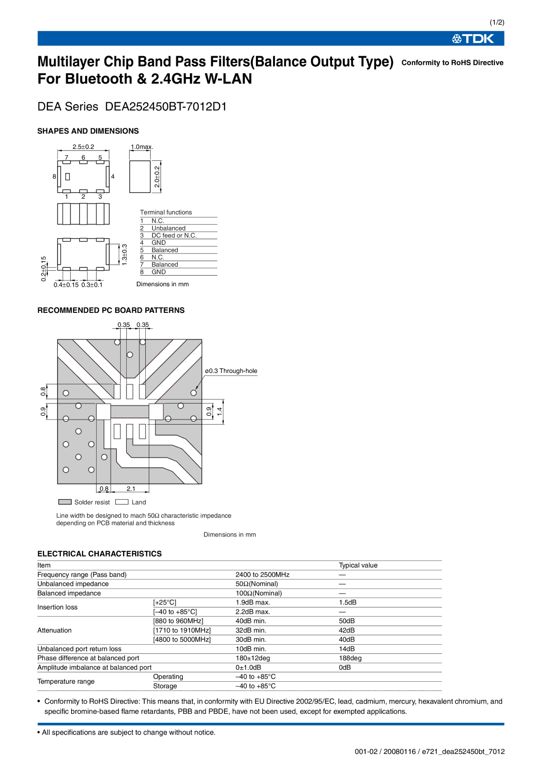
SHAPES AND DIMENSIONS
2.5±0.2
7 6 5
8
4
1.0max.
2.0±0.2
1 2 3
0.15 | 1.3±0.3 |
0.2± | 0.4±0.15 0.3±0.1 |
|
Terminal functions
1N.C.
2Unbalanced
3DC feed or N.C.
4GND
5Balanced
6N.C.
7Balanced
8GND
Dimensions in mm
RECOMMENDED PC BOARD PATTERNS
| 0.35 | 0.35 |
|
|
| ø0.3 | |
0.8 |
|
|
|
0.9 |
| 0.9 | 1.4 |
0.8 | 2.1 |
| |
Solder resist |
| Land |
|
Line width be designed to mach 50Ω characteristic impedance depending on PCB material and thickness
Dimensions in mm
ELECTRICAL CHARACTERISTICS
Item |
|
| Typical value | |
Frequency range (Pass band) |
| 2400 to 2500MHz | — | |
Unbalanced impedance |
| 50Ω(Nominal) | — | |
Balanced impedance |
| 100Ω(Nominal) | — | |
Insertion loss | [+25°C] | 1.9dB max. | 1.5dB | |
2.2dB max. | — | |||
| ||||
| [880 to 960MHz] | 40dB min. | 50dB | |
Attenuation | [1710 to 1910MHz] | 32dB min. | 42dB | |
| [4800 to 5000MHz] | 30dB min. | 40dB | |
Unbalanced port return loss |
| 10dB min. | 14dB | |
Phase difference at balanced port |
| 180±12deg | 188deg | |
Amplitude imbalance at balanced port |
| 0±1.0dB | 0dB | |
Temperature range | Operating |
| ||
Storage |
| |||
|
|
•Conformity to RoHS Directive: This means that, in conformity with EU Directive 2002/95/EC, lead, cadmium, mercury, hexavalent chromium, and specific
•All specifications are subject to change without notice.
