www.ti.com
EVM Bill of Materials, Assembly Drawing, and Schematic
The digital control signals can be applied directly to J1 and J5 (top or bottom side). The ADS8364/65MEVM can also be connected directly to the
The BYTE signal, which controls the output of the ADS836x when used with
The conversion clock can be applied to J7, a BNC connector with a
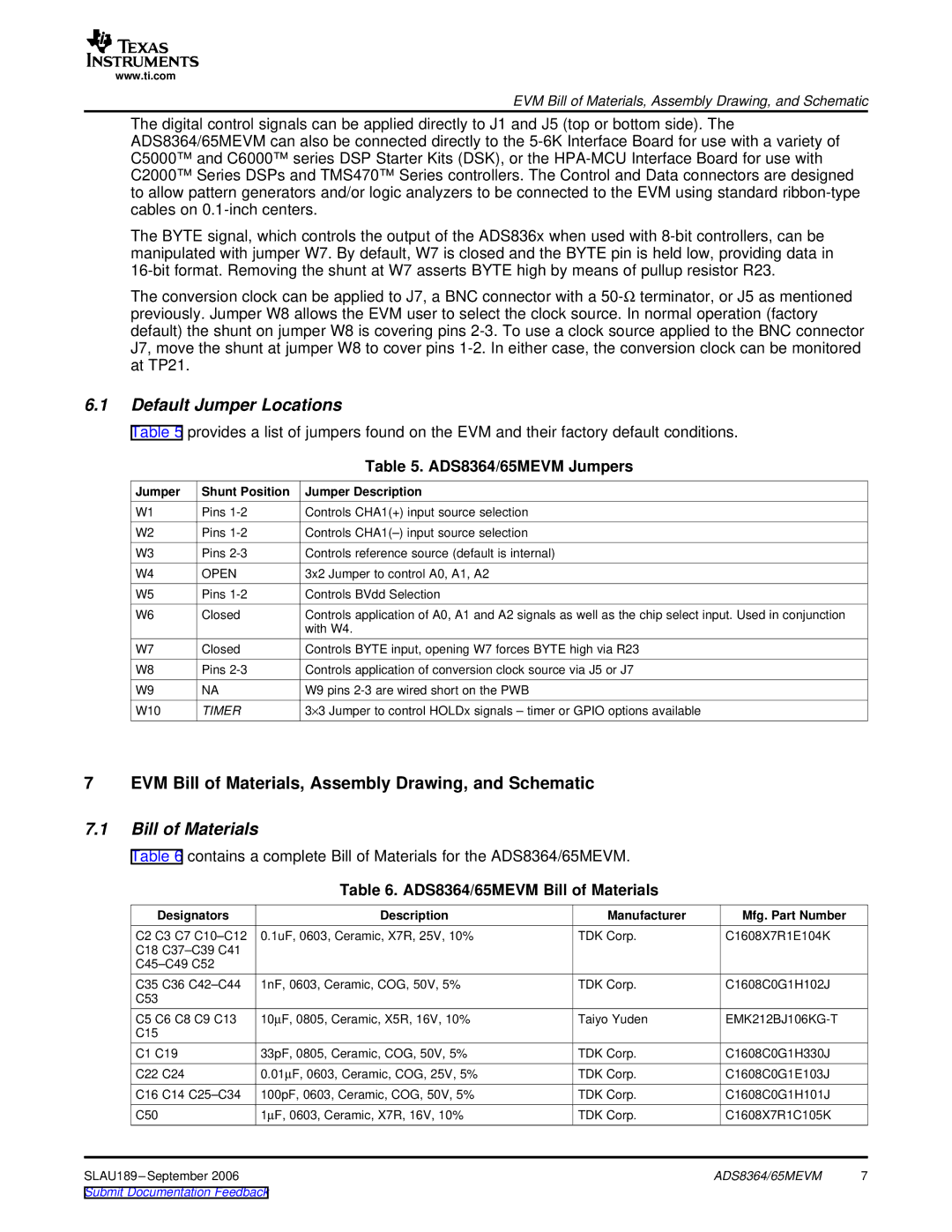
6.1Default Jumper Locations
Table 5 provides a list of jumpers found on the EVM and their factory default conditions.
|
| Table 5. ADS8364/65MEVM Jumpers |
Jumper | Shunt Position | Jumper Description |
W1 | Pins | Controls CHA1(+) input source selection |
W2 | Pins | Controls |
W3 | Pins | Controls reference source (default is internal) |
W4 | OPEN | 3x2 Jumper to control A0, A1, A2 |
W5 | Pins | Controls BVdd Selection |
W6 | Closed | Controls application of A0, A1 and A2 signals as well as the chip select input. Used in conjunction |
|
| with W4. |
W7 | Closed | Controls BYTE input, opening W7 forces BYTE high via R23 |
W8 | Pins | Controls application of conversion clock source via J5 or J7 |
W9 | NA | W9 pins |
W10 | TIMER | 3×3 Jumper to control HOLDx signals – timer or GPIO options available |
7 EVM Bill of Materials, Assembly Drawing, and Schematic
7.1Bill of Materials
Table 6 contains a complete Bill of Materials for the ADS8364/65MEVM.
Table 6. ADS8364/65MEVM Bill of Materials
Designators | Description | Manufacturer | Mfg. Part Number |
| |
C2 C3 C7 | 0.1uF, 0603, Ceramic, X7R, 25V, 10% | TDK Corp. | C1608X7R1E104K |
| |
C18 |
|
|
|
| |
|
|
|
| ||
C35 | C36 | 1nF, 0603, Ceramic, COG, 50V, 5% | TDK Corp. | C1608C0G1H102J |
|
C53 |
|
|
|
|
|
C5 C6 C8 C9 C13 | 10μF, 0805, Ceramic, X5R, 16V, 10% | Taiyo Yuden |
| ||
C15 |
|
|
|
|
|
C1 C19 | 33pF, 0805, Ceramic, COG, 50V, 5% | TDK Corp. | C1608C0G1H330J |
| |
C22 | C24 | 0.01μF, 0603, Ceramic, COG, 25V, 5% | TDK Corp. | C1608C0G1E103J |
|
C16 | C14 | 100pF, 0603, Ceramic, COG, 50V, 5% | TDK Corp. | C1608C0G1H101J |
|
C50 |
| 1μF, 0603, Ceramic, X7R, 16V, 10% | TDK Corp. | C1608X7R1C105K |
|
SLAU189 |
|
| ADS8364/65MEVM | 7 | |
Submit Documentation Feedback |
|
|
| ||