www.ti.com
Digital Interface
The output from the buffer stage in each case applies 0-5 V to the CHA0(+) input when the applied signal is connected to J2 pin 1 or J4 pin 2. The applied signal is directed to the CHA0(-) input when connected via J2 pin 3 or J4 pin 4.
When operating the ADS836x with single-ended signals, it is important to keep the unused ADC input biased to +2.5 V. This is easily accomplished on the EVM by changing the components associated with either the inverting or noninverting input only, leaving the default component values shown in Table 1 on the unused input. For example, to achieve a bipolar input range of ±10 V on CHA0(+), use the component values shown for R1–R4 and move the shunt on W2 position 2-3. Components R24, R25, R28, and R29 and the shunt on W1 should remain in the default conditions shown in Table 1.
3.3Analog Input – Channel A1
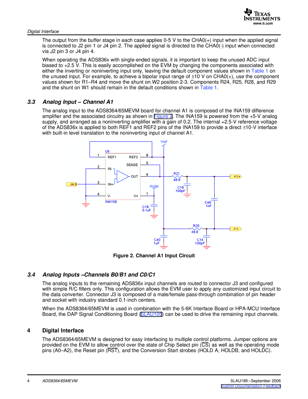
The analog input to the ADS8364/65MEVM board for channel A1 is composed of the INA159 difference amplifier and the associated circuitry as shown in Figure 2. The INA159 is powered from the +5-V analog
supply, and arranged as a noninverting amplifier with a gain of 0.2. The internal +2.5-V reference voltage of the ADS836x is applied to both REF1 and REF2 pins of the INA159 to provide a direct ±10-V interface with built-in level translation to the noninverting input of channel A1.
Figure 2. Channel A1 Input Circuit
3.4Analog Inputs –Channels B0/B1 and C0/C1
The analog inputs to the remaining ADS836x input channels are routed to connector J3 and configured with simple R/C filters only. This configuration allows the EVM user to apply any customized input circuit to the data converter. Connector J3 is composed of a male/female pass-through combination of pin header and socket with industry standard 0.1-inch centers.
When the ADS8364/65MEVM is used in combination with the 5-6K Interface Board or HPA-MCU Interface Board, the DAP Signal Conditioning Board (SLAU105) can be used to drive the remaining input channels.
4Digital Interface
The ADS8364/65MEVM is designed for easy interfacing to multiple control platforms. Jumper options are provided on the EVM to allow control over the state of Chip Select pin (CS) as well as the operating mode pins (A0–A2), the Reset pin (RST), and the Conversion Start strobes (HOLD A, HOLDB, and HOLDC).
4 | ADS8364/65MEVM | SLAU189 –September 2006 |