www.ti.com
Power Supplies
|
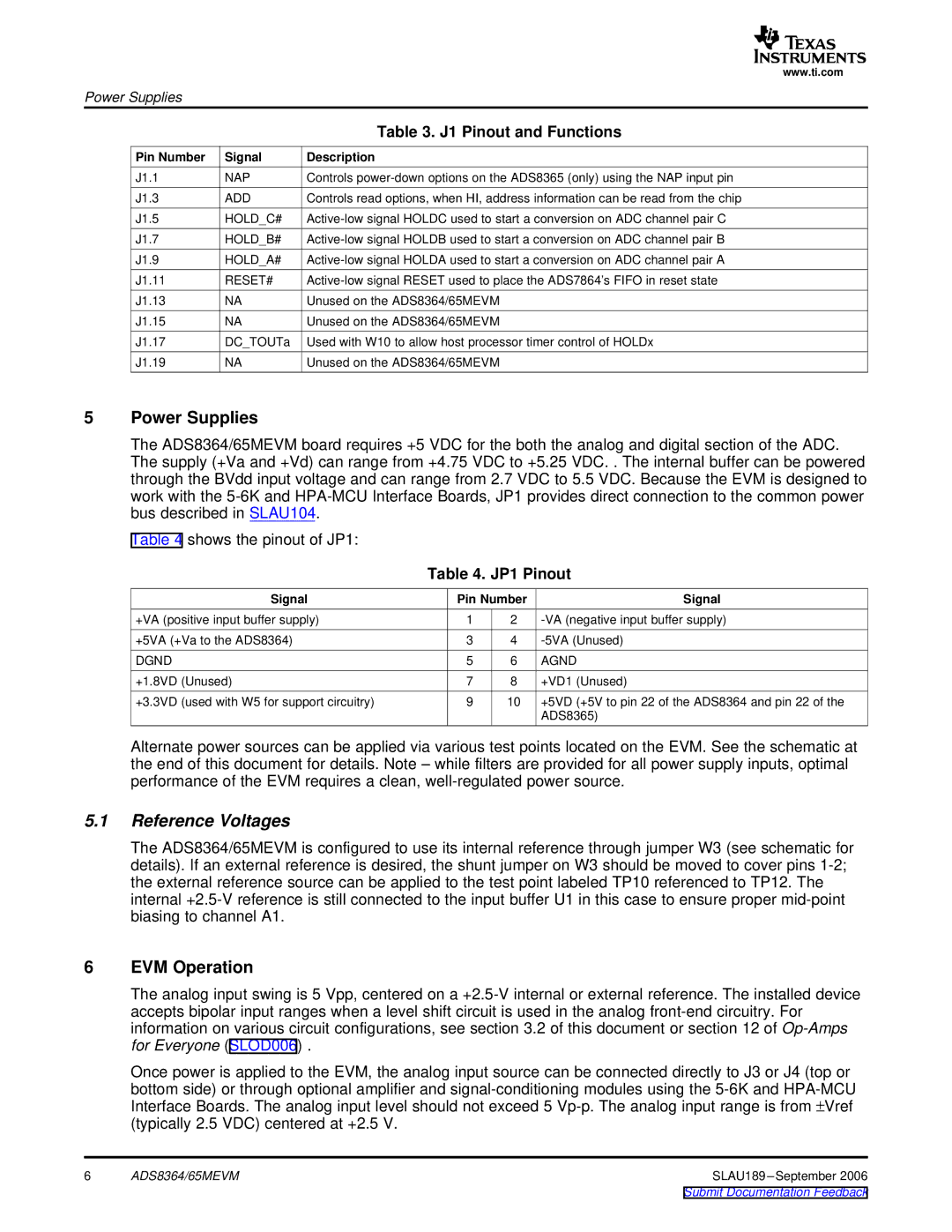
| Table 3. J1 Pinout and Functions |
Pin Number | Signal | Description |
J1.1 | NAP | Controls |
J1.3 | ADD | Controls read options, when HI, address information can be read from the chip |
J1.5 | HOLD_C# | |
J1.7 | HOLD_B# | |
J1.9 | HOLD_A# | |
J1.11 | RESET# | |
J1.13 | NA | Unused on the ADS8364/65MEVM |
J1.15 | NA | Unused on the ADS8364/65MEVM |
J1.17 | DC_TOUTa | Used with W10 to allow host processor timer control of HOLDx |
J1.19 | NA | Unused on the ADS8364/65MEVM |
5Power Supplies
The ADS8364/65MEVM board requires +5 VDC for the both the analog and digital section of the ADC. The supply (+Va and +Vd) can range from +4.75 VDC to +5.25 VDC. . The internal buffer can be powered through the BVdd input voltage and can range from 2.7 VDC to 5.5 VDC. Because the EVM is designed to work with the
Table 4 shows the pinout of JP1:
Table 4. JP1 Pinout
Signal | Pin Number | Signal | |
+VA (positive input buffer supply) | 1 | 2 | |
+5VA (+Va to the ADS8364) | 3 | 4 | |
DGND | 5 | 6 | AGND |
+1.8VD (Unused) | 7 | 8 | +VD1 (Unused) |
+3.3VD (used with W5 for support circuitry) | 9 | 10 | +5VD (+5V to pin 22 of the ADS8364 and pin 22 of the |
|
|
| ADS8365) |
Alternate power sources can be applied via various test points located on the EVM. See the schematic at the end of this document for details. Note – while filters are provided for all power supply inputs, optimal performance of the EVM requires a clean,
5.1Reference Voltages
The ADS8364/65MEVM is configured to use its internal reference through jumper W3 (see schematic for details). If an external reference is desired, the shunt jumper on W3 should be moved to cover pins
6EVM Operation
The analog input swing is 5 Vpp, centered on a
Once power is applied to the EVM, the analog input source can be connected directly to J3 or J4 (top or
bottom side) or through optional amplifier and
6 | ADS8364/65MEVM | SLAU189 |
Submit Documentation Feedback
