Manuals
/
Texas Instruments
/
Computer Equipment
/
Switch
Texas Instruments
HPL-D SLLU064A Board Layout Patterns, X4 Crosspoint Switch EVM Board Layout
Models:
HPL-D SLLU064A
1
21
27
27
Download
27 pages
55.11 Kb
18
19
20
21
22
23
24
25
Schematic
Signal Paths
Setup and Required Equipment
X4 Crosspoint Switch EVM
Page 21
Image 21
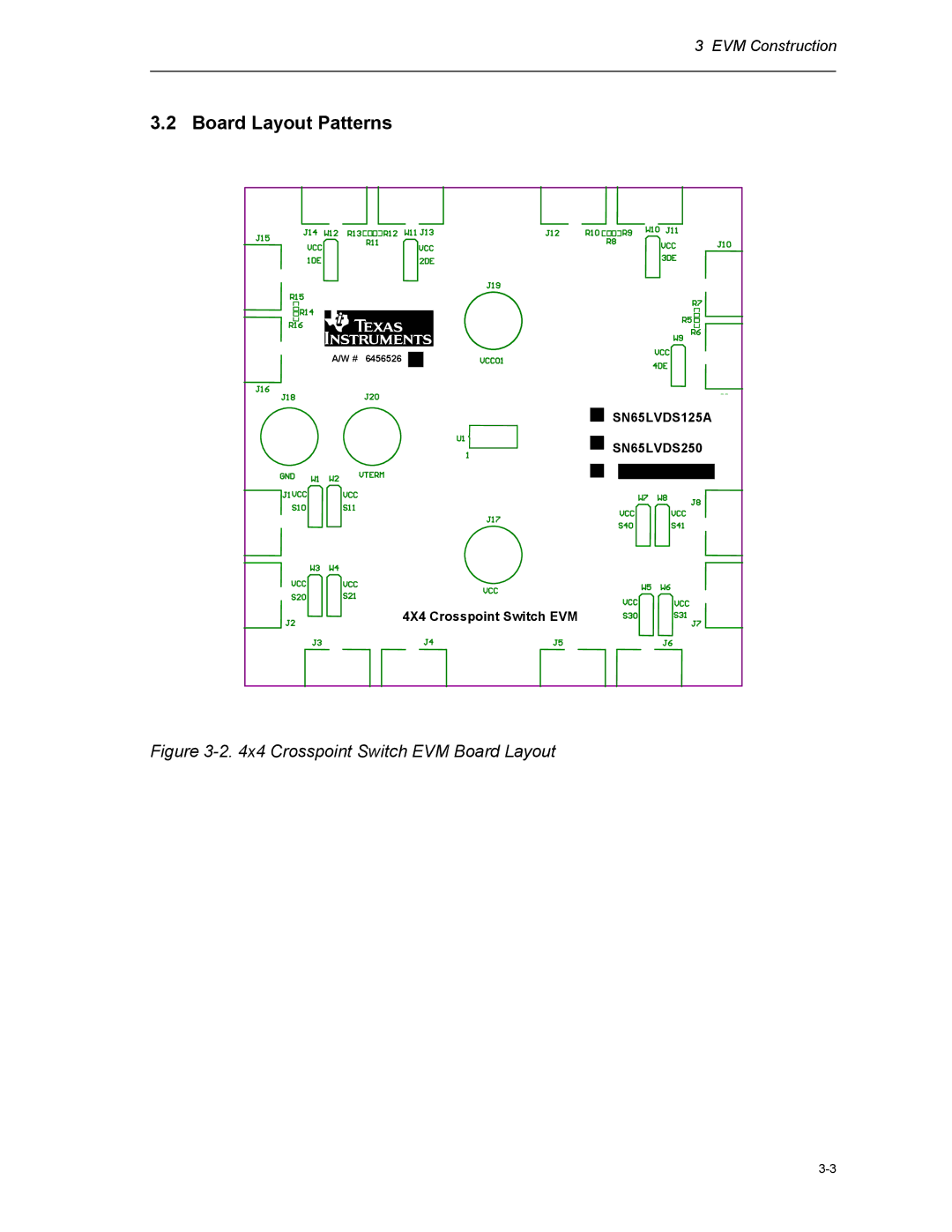
3 EVM Construction
3.2 Board Layout Patterns
A/W
#
6456526
SN65
L
VDS125A
SN65LVDS250
4X4 Crosspoint Switch EVM
Figure
3-2.
4x4 Crosspoint Switch EVM Board Layout
3-3
Page 20
Page 22
Page 21
Image 21
Page 20
Page 22
Contents
Users Guide
Important Notice
EVM Important Notice
EVM Warnings and Restrictions
About This Manual
Read This First
FCC Warning
Figures
Contents
Tables
Overview
Sample Functional Configurations
X4 Crosspoint Switch EVM
X4 Crosspoint Switch Signal Paths
Signal Paths
Applying an Input
Setup and Required Equipment
Setup and Required Equipment
Termination for Interfacing LVDS, CML, or Lvpecl Drivers
Typical Test Results
Observing an Output
Typical Test Results
Setup and Required Equipment
EVM Construction
X4 Crosspoint Switch EVM Schematic
Schematic
Board Layout Patterns
X4 Crosspoint Switch EVM Board Layout
Layer 1-Signal Plane
GND Plane
Layer 4-Vcc01 Plane
Layer 6-GND/Signal Plane
PCB Fabrication Requirements and Stack Up
Bill of Materials for SN65LVDS125A / SN65LVDS250 EVM
Bill of Materials
Top
Page
Image
Contents