Interface Circuit
2.2 Interface Circuit
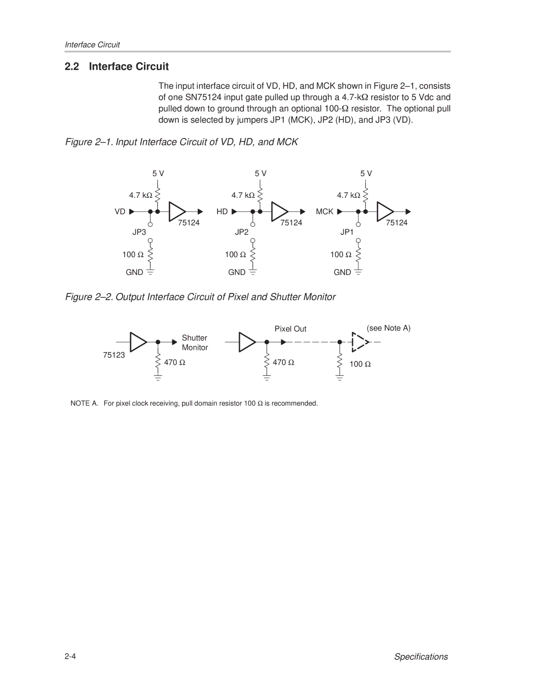
The input interface circuit of VD, HD, and MCK shown in Figure 2±1, consists of one SN75124 input gate pulled up through a
Figure 2±1. Input Interface Circuit of VD, HD, and MCK
5 V | 5 V | 5 V |
4.7 kΩ | 4.7 kΩ | 4.7 kΩ |
VD | HD | MCK |
75124 | 75124 | 75124 |
JP3 | JP2 | JP1 |
100 Ω | 100 Ω | 100 Ω |
GND | GND | GND |
Figure 2±2. Output Interface Circuit of Pixel and Shutter Monitor
| Shutter | Pixel Out | (see Note A) |
|
|
| |
75123 | Monitor |
|
|
Ω | 470 Ω |
| |
470 | 100 Ω |
NOTE A. For pixel clock receiving, pull domain resistor 100 Ω is recommended.
Specifications |