Registers | www.ti.com |
3.4CMPUDAT
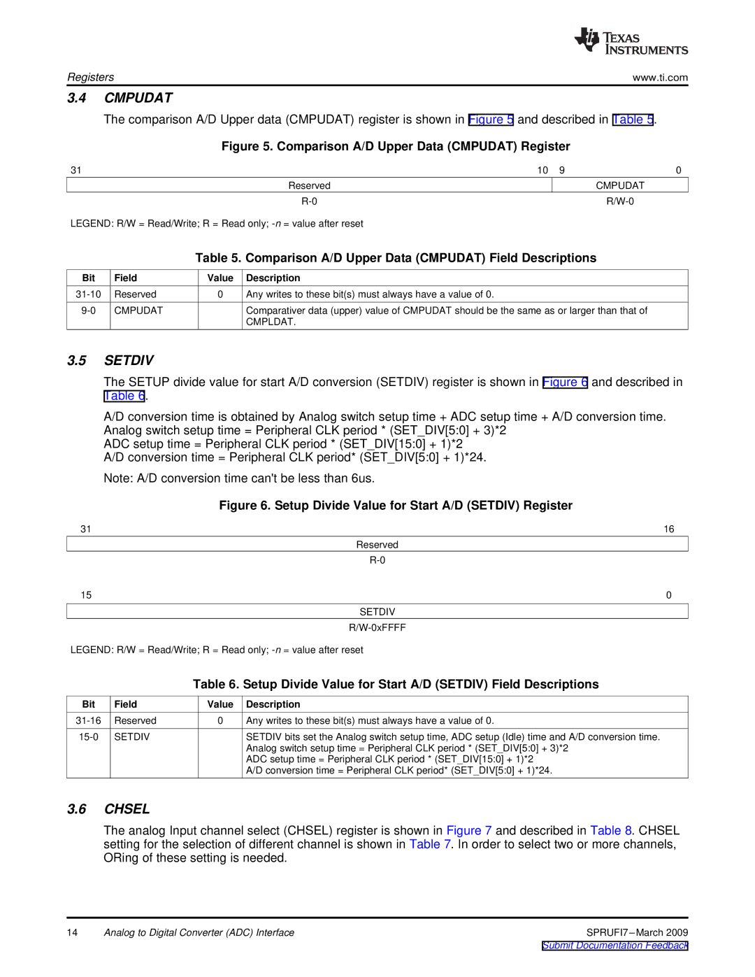
The comparison A/D Upper data (CMPUDAT) register is shown in Figure 5 and described in Table 5.
Figure 5. Comparison A/D Upper Data (CMPUDAT) Register
31 | 10 | 9 | 0 |
Reserved |
|
| CMPUDAT |
|
|
LEGEND: R/W = Read/Write; R = Read only;
Table 5. Comparison A/D Upper Data (CMPUDAT) Field Descriptions
Bit | Field | Value | Description |
Reserved | 0 | Any writes to these bit(s) must always have a value of 0. | |
CMPUDAT |
| Comparativer data (upper) value of CMPUDAT should be the same as or larger than that of | |
|
|
| CMPLDAT. |
3.5SETDIV
The SETUP divide value for start A/D conversion (SETDIV) register is shown in Figure 6 and described in Table 6.
A/D conversion time is obtained by Analog switch setup time + ADC setup time + A/D conversion time. Analog switch setup time = Peripheral CLK period * (SET_DIV[5:0] + 3)*2
ADC setup time = Peripheral CLK period * (SET_DIV[15:0] + 1)*2 A/D conversion time = Peripheral CLK period* (SET_DIV[5:0] + 1)*24.
Note: A/D conversion time can't be less than 6us.
|
| Figure 6. Setup Divide Value for Start A/D (SETDIV) Register | |
31 |
|
| 16 |
|
|
| Reserved |
|
|
| |
15 |
|
| 0 |
|
|
| SETDIV |
|
|
| |
LEGEND: R/W = Read/Write; R = Read only; | |||
|
| Table 6. Setup Divide Value for Start A/D (SETDIV) Field Descriptions | |
Bit | Field | Value | Description |
Reserved | 0 | Any writes to these bit(s) must always have a value of 0. | |
SETDIV |
| SETDIV bits set the Analog switch setup time, ADC setup (Idle) time and A/D conversion time. | |
|
|
| Analog switch setup time = Peripheral CLK period * (SET_DIV[5:0] + 3)*2 |
|
|
| ADC setup time = Peripheral CLK period * (SET_DIV[15:0] + 1)*2 |
|
|
| A/D conversion time = Peripheral CLK period* (SET_DIV[5:0] + 1)*24. |
3.6CHSEL
The analog Input channel select (CHSEL) register is shown in Figure 7 and described in Table 8. CHSEL setting for the selection of different channel is shown in Table 7. In order to select two or more channels, ORing of these setting is needed.
14 | Analog to Digital Converter (ADC) Interface |
