Registers | www.ti.com |
3.1ADCTL
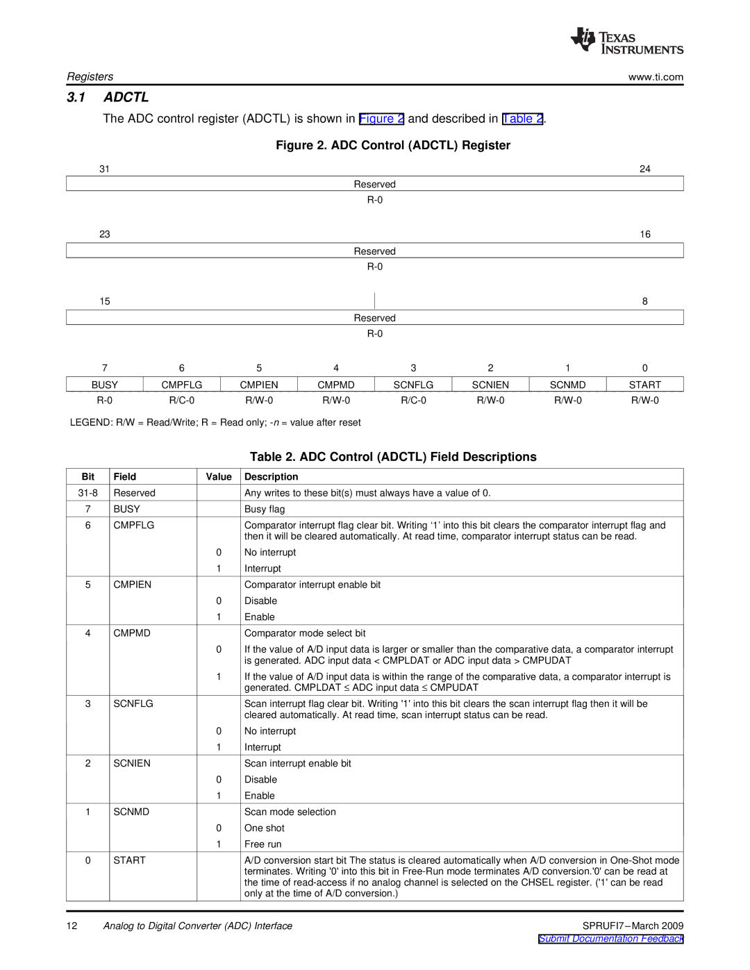
The ADC control register (ADCTL) is shown in Figure 2 and described in Table 2.
|
|
|
| Figure 2. ADC Control (ADCTL) Register |
|
| |||
| 31 |
|
|
|
|
|
|
| 24 |
|
|
|
|
| Reserved |
|
|
| |
|
|
|
|
|
|
|
|
| |
| 23 |
|
|
|
|
|
|
| 16 |
|
|
|
|
| Reserved |
|
|
| |
|
|
|
|
|
|
|
|
| |
| 15 |
|
|
|
|
|
|
| 8 |
|
|
|
|
| Reserved |
|
|
| |
|
|
|
|
|
|
|
|
| |
| 7 |
| 6 | 5 | 4 | 3 | 2 | 1 | 0 |
| BUSY | CMPFLG | CMPIEN | CMPMD | SCNFLG | SCNIEN | SCNMD | START | |
|
| ||||||||
LEGEND: R/W = Read/Write; R = Read only; |
|
|
|
| |||||
|
|
|
| Table 2. ADC Control (ADCTL) Field Descriptions |
|
| |||
| Bit | Field | Value | Description |
|
|
|
|
|
| Reserved |
| Any writes to these bit(s) must always have a value of 0. |
|
| ||||
| 7 | BUSY |
| Busy flag |
|
|
|
|
|
| 6 | CMPFLG |
| Comparator interrupt flag clear bit. Writing ‘1’ into this bit clears the comparator interrupt flag and | |||||
|
|
|
| then it will be cleared automatically. At read time, comparator interrupt status can be read. | |||||
|
|
| 0 | No interrupt |
|
|
|
|
|
|
|
| 1 | Interrupt |
|
|
|
|
|
| 5 | CMPIEN |
| Comparator interrupt enable bit |
|
|
|
| |
|
|
| 0 | Disable |
|
|
|
|
|
|
|
| 1 | Enable |
|
|
|
|
|
| 4 | CMPMD |
| Comparator mode select bit |
|
|
|
| |
|
|
| 0 | If the value of A/D input data is larger or smaller than the comparative data, a comparator interrupt | |||||
|
|
|
| is generated. ADC input data < CMPLDAT or ADC input data > CMPUDAT |
| ||||
|
|
| 1 | If the value of A/D input data is within the range of the comparative data, a comparator interrupt is | |||||
|
|
|
| generated. CMPLDAT ≤ ADC input data ≤ CMPUDAT |
|
| |||
| 3 | SCNFLG |
| Scan interrupt flag clear bit. Writing '1' into this bit clears the scan interrupt flag then it will be | |||||
|
|
|
| cleared automatically. At read time, scan interrupt status can be read. |
|
| |||
|
|
| 0 | No interrupt |
|
|
|
|
|
|
|
| 1 | Interrupt |
|
|
|
|
|
| 2 | SCNIEN |
| Scan interrupt enable bit |
|
|
|
| |
|
|
| 0 | Disable |
|
|
|
|
|
|
|
| 1 | Enable |
|
|
|
|
|
| 1 | SCNMD |
| Scan mode selection |
|
|
|
| |
|
|
| 0 | One shot |
|
|
|
|
|
|
|
| 1 | Free run |
|
|
|
|
|
| 0 | START |
| A/D conversion start bit The status is cleared automatically when A/D conversion in | |||||
|
|
|
| terminates. Writing '0' into this bit in | |||||
|
|
|
| the time of | |||||
|
|
|
| only at the time of A/D conversion.) |
|
|
| ||
12 | Analog to Digital Converter (ADC) Interface |
|
|
| |||||
