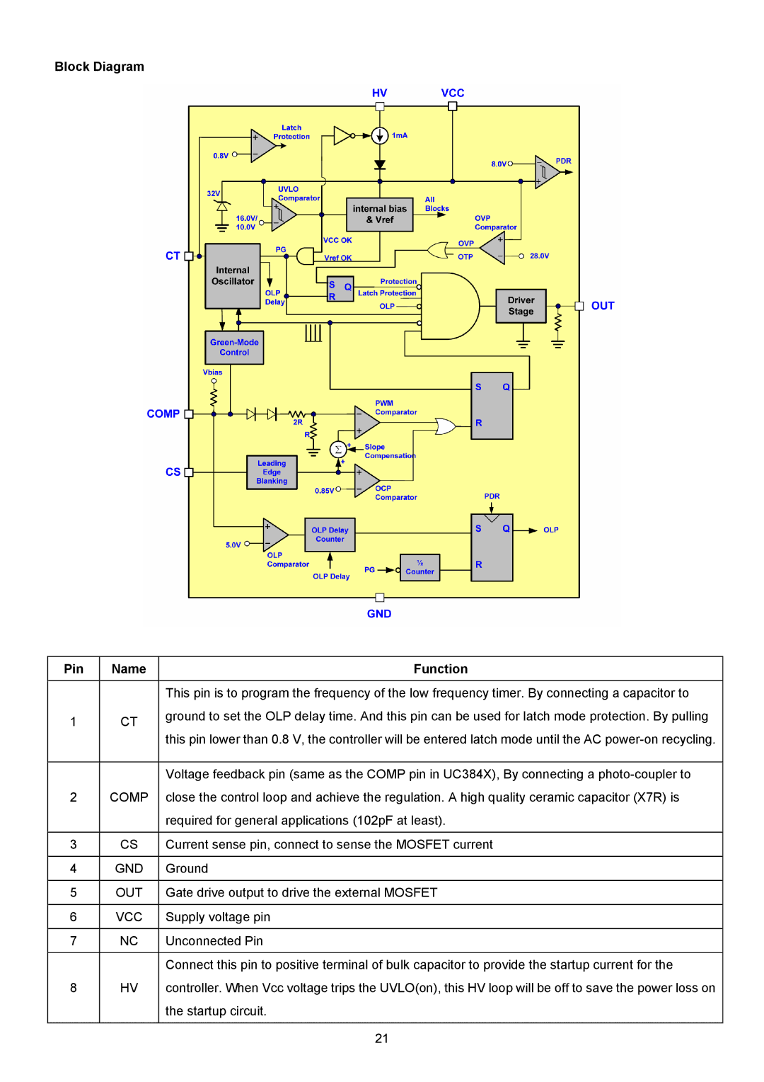
Block Diagram
Pin | Name |
1CT
2COMP
3CS
4GND
5OUT
6VCC
7NC
8HV
Function
This pin is to program the frequency of the low frequency timer. By connecting a capacitor to ground to set the OLP delay time. And this pin can be used for latch mode protection. By pulling this pin lower than 0.8 V, the controller will be entered latch mode until the AC
Voltage feedback pin (same as the COMP pin in UC384X), By connecting a
Current sense pin, connect to sense the MOSFET current
Ground
Gate drive output to drive the external MOSFET
Supply voltage pin
Unconnected Pin
Connect this pin to positive terminal of bulk capacitor to provide the startup current for the controller. When Vcc voltage trips the UVLO(on), this HV loop will be off to save the power loss on the startup circuit.
21