Manuals
/
ViewSonic
/
TV and Video
/
Flat Panel Television
ViewSonic
VSXXXXX
service manual
PCB Layout Diagrams, Main Board
Models:
VSXXXXX
1
44
67
67
Download
67 pages
38.06 Kb
41
42
43
44
45
46
47
48
Troubleshooting
Specifications
Install
Parts list
Block Diagram Pin
Jumper Wire
Connector
Adjustment Procedure
Audio Adjust
Precautions and Safety Notices
Page 44
Image 44
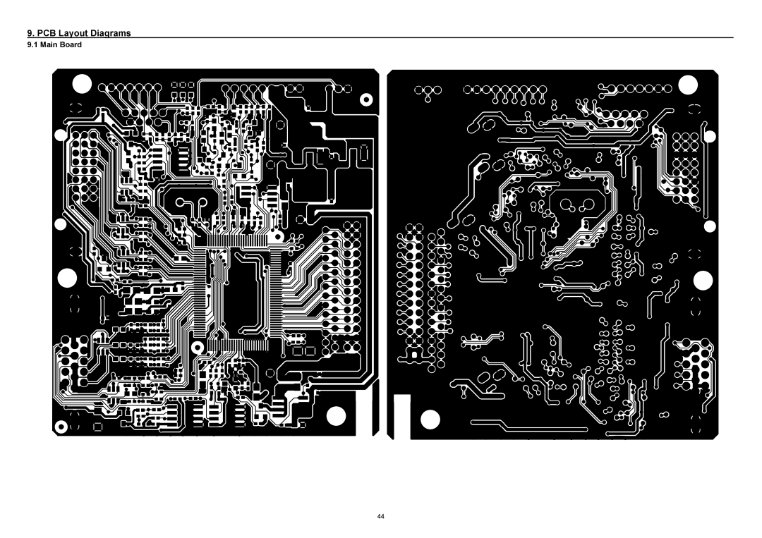
9. PCB Layout Diagrams
9.1 Main Board
44
Page 43
Page 45
Page 44
Image 44
Page 43
Page 45
Contents
ViewSonic VG2427wm
VG2427wmSM Rev a Mar
Tdrmnddkwbvspc
Tdrmnddywbvspc
Tdrmnddcwbvspc
Tdrmnddbwbvspc
Table of Contents
Precautions and Safety Notices
Safety Precautions
Product Safety Notice
Service Notes
Handing and Placing Methods
Correct Methods Incorrect Methods
Page
Specification
Front Panel Function Control Description
Do the following to adjust the display setting
Following tips may help you optimize your display
Control Explanation
Audio Adjust
Main Menu Controls
Page
Page
Circuit Description
Main Board
Pin Assignment
Page
Page
Page
Page
Function
Pin Descriptions
Name Pin #
Power Board
Typical Application
Block Diagram Pin
Comp GND OUT VCC
Pin Diagram Functional Block Diagram
IC801 TA9687GN
Pin Description Pin No Names
Adjustment Procedure
White balance, Luminance adjustment
Enter into Burn/in mode
Enter into the factory mode
Equipment needed
Firmware Upgrade Procedure
ISP Board
Hardware Connect status Update the NOVATEK’S firmware
PC LPT
Page
Page
DDC Key in Procedure
Install software
For analog
Page
Troubleshooting Flow Chart
Block Diagram
DIM
ON/OFF
Mosfet
Schematic Diagrams
0R05 1/10W 5%
FB402
TO252
0402
Power Board
Power XFMR7
IC with Heat-sink90G6295-3
PCB Name
Key Board
TPV Model
USB Board
Upstream
PCB Layout Diagrams
Page
Power Board
Page
Key Board USB Board
Page
Exploded Diagram and Exploded Parts List
10.1 EPL
Description Part Number Qty
10.2 PPL
Recommended Spare Parts List
Location Part Number Description Remark
Cbpc Label
Wafer
CONN.6P 1.0 DIP
Wafer 30P 2.0MM DIP Dual ROW
Page
Chip 22PF 50V NPO
RST Chip MAX
RST Chipr
Chip 5PF 50V NPO
Bead 300Ω
Chip Bead
Chip Bead FCM2012VF-301T07 Bullwill
Dome Switch 5PCS
PIN PWPC9D41MQWU Power Board
UDZSNP5.6B Rohm
TRA LMBT3904LT1G 200MA/40V SOT-23 LRC
IC PC123Y22FZ0F
RST Ntcr 8OHM £«£20£¥ 4A Xianzheng
CAP CER 56PF J 3KV
Choke by LI TA
Screw HS1
Heat Sink
Diode SP1060 ITO-220 Secos
Screw HS2
RST Chipr 3.6K
RST Chipr 6.2KOHM +-5% 1/10W Yageo
1ST Chipr
RST Chipr 1K
NPO
RST Chipr 820KOHM +-5% 1/4W Fenghua
X7R
Power Board PCB
Jumper Wire
Chip Bead HCB3216KF-800T30 Bullwill
BAV70 SOT23 by PAN JIT
Connector
VSC 23.6 Hinge Assy
HT POT Label
Pallet Label
RST Chip MAX 0R05 1/4W
Diode ESD EGA 10603V05A1-B Inpaq
USB Board PCB
Different Parts List
Diversity of Tdrmnddcwbvspc compared with Tdrmnddkwbvspc
Location Part Number Description
Diversity of Tdrmnddbwbvspc compared with Tdrmnddkwbvspc
Reader’s Response
Name Company Add Tel Mail Title Fax
Top
Page
Image
Contents