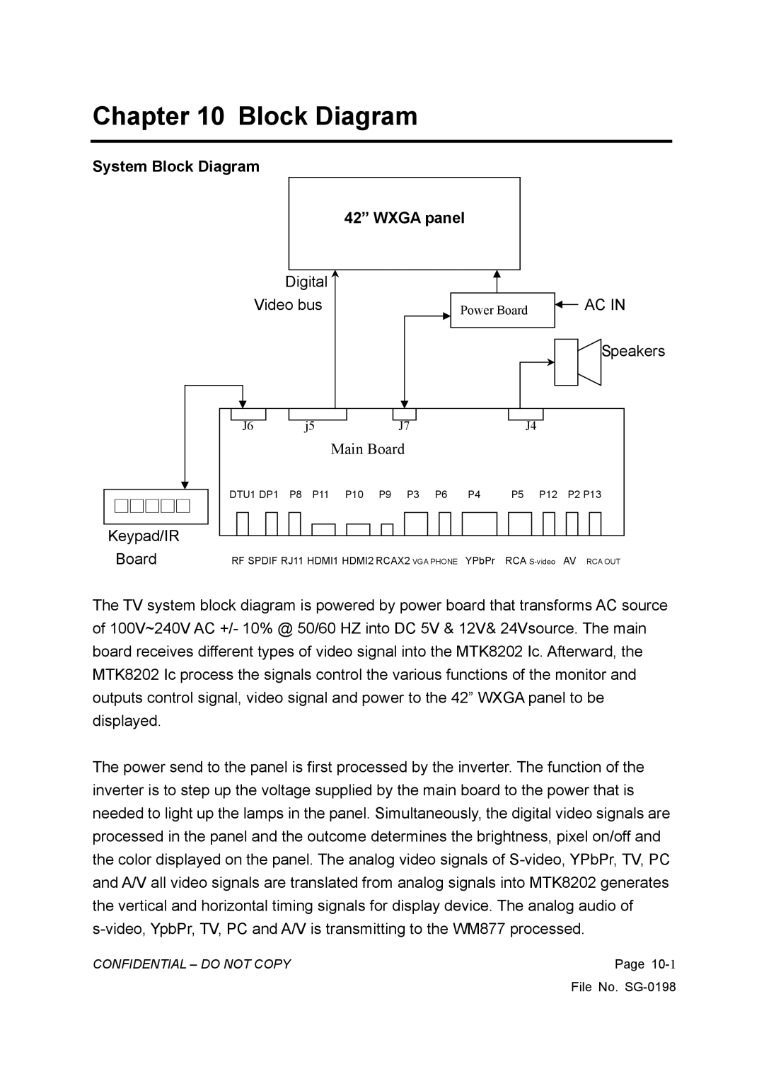
Chapter 10 Block Diagram
System Block Diagram
42” WXGA panel
Digital Video bus
Power Board | AC IN |
|
|
Speakers
□□□□□
Keypad/IR
Board
|
|
|
|
|
|
|
|
|
|
|
|
|
|
|
|
|
|
|
|
|
|
|
|
|
|
|
|
|
|
| J6 |
| j5 |
|
|
|
|
| J7 |
|
|
|
|
|
| J4 | |||||||||||||
|
|
|
|
|
|
|
|
| Main Board |
|
|
|
|
|
|
|
| ||||||||||||
DTU1 DP1 | P8 P11 |
| P10 P9 P3 P6 P4 | P5 P12 P2 P13 | |||||||||||||||||||||||||
|
|
|
|
|
|
|
|
|
|
|
|
|
|
|
|
|
|
|
|
|
|
|
|
|
|
|
|
|
|
|
|
|
|
|
|
|
|
|
|
|
|
|
|
|
|
|
|
|
|
|
|
|
|
|
|
|
|
|
|
|
|
|
|
|
|
|
|
|
|
|
|
|
|
|
|
|
|
|
|
|
|
|
|
|
|
|
|
|
|
RF SPDIF RJ11 HDMI1 HDMI2 RCAX2 VGA PHONE YPbPr RCA
The TV system block diagram is powered by power board that transforms AC source of 100V~240V AC +/- 10% @ 50/60 HZ into DC 5V & 12V& 24Vsource. The main board receives different types of video signal into the MTK8202 Ic. Afterward, the MTK8202 Ic process the signals control the various functions of the monitor and outputs control signal, video signal and power to the 42” WXGA panel to be displayed.
The power send to the panel is first processed by the inverter. The function of the inverter is to step up the voltage supplied by the main board to the power that is needed to light up the lamps in the panel. Simultaneously, the digital video signals are processed in the panel and the outcome determines the brightness, pixel on/off and the color displayed on the panel. The analog video signals of
CONFIDENTIAL – DO NOT COPY | Page |
| File No. |