4. Bank Activate Command
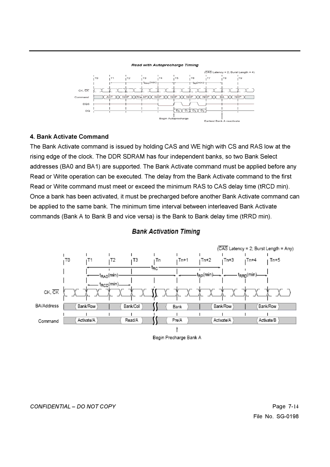
The Bank Activate command is issued by holding CAS and WE high with CS and RAS low at the rising edge of the clock. The DDR SDRAM has four independent banks, so two Bank Select addresses (BA0 and BA1) are supported. The Bank Activate command must be applied before any Read or Write operation can be executed. The delay from the Bank Activate command to the first Read or Write command must meet or exceed the minimum RAS to CAS delay time (tRCD min). Once a bank has been activated, it must be precharged before another Bank Activate command can be applied to the same bank. The minimum time interval between interleaved Bank Activate commands (Bank A to Bank B and vice versa) is the Bank to Bank delay time (tRRD min).
CONFIDENTIAL – DO NOT COPY | Page |
| File No. |
