QUIESCENT CONDITION:
This design is class A/B and therefore the output driver transistors must be forward biased to provide low crossover distortion. In most class A/B designs, a diode chain or VBE multiplier is used to control the bias voltage and provide a means of adjusting the bias. This design is different as there isn't a diode chain or VBE multiplier. For simplicity lets consider only the positive side of the current amplifier, that is all parts between the positive power supply rails and the audio signal output/input terminals. The negative side is the same as the positive, except for polarity changes.
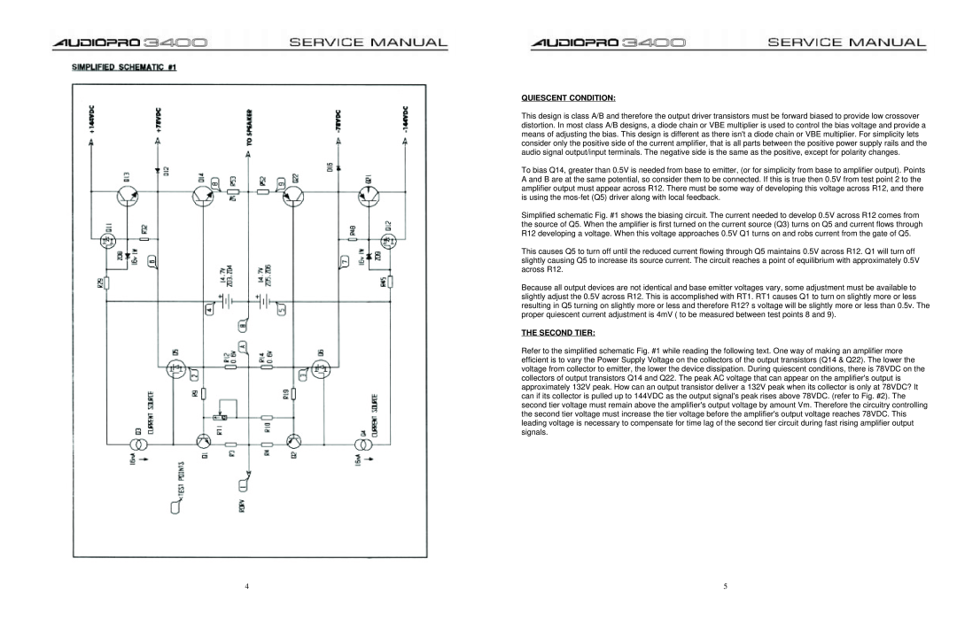
To bias Q14, greater than 0.5V is needed from base to emitter, (or for simplicity from base to amplifier output). Points A and B are at the same potential, so consider them to be connected. If this is true then 0.5V from test point 2 to the amplifier output must appear across R12. There must be some way of developing this voltage across R12, and there is using the
Simplified schematic Fig. #1 shows the biasing circuit. The current needed to develop 0.5V across R12 comes from the source of Q5. When the amplifier is first turned on the current source (Q3) turns on Q5 and current flows through R12 developing a voltage. When this voltage approaches 0.5V Q1 turns on and robs current from the gate of Q5.
This causes Q5 to turn off until the reduced current flowing through Q5 maintains 0.5V across R12. Q1 will turn off slightly causing Q5 to increase its source current. The circuit reaches a point of equilibrium with approximately 0.5V across R12.
Because all output devices are not identical and base emitter voltages vary, some adjustment must be available to slightly adjust the 0.5V across R12. This is accomplished with RT1. RT1 causes Q1 to turn on slightly more or less resulting in Q5 turning on slightly more or less and therefore R12? s voltage will be slightly more or less than 0.5v. The proper quiescent current adjustment is 4mV ( to be measured between test points 8 and 9).
THE SECOND TIER:
Refer to the simplified schematic Fig. #1 while reading the following text. One way of making an amplifier more efficient is to vary the Power Supply Voltage on the collectors of the output transistors (Q14 & Q22). The lower the voltage from collector to emitter, the lower the device dissipation. During quiescent conditions, there is 78VDC on the collectors of output transistors Q14 and Q22. The peak AC voltage that can appear on the amplifier's output is approximately 132V peak. How can an output transistor deliver a 132V peak when its collector is only at 78VDC? It can if its collector is pulled up to 144VDC as the output signal's peak rises above 78VDC. (refer to Fig. #2). The second tier voltage must remain above the amplifier's output voltage by amount Vm. Therefore the circuitry controlling the second tier voltage must increase the tier voltage before the amplifier's output voltage reaches 78VDC. This leading voltage is necessary to compensate for time lag of the second tier circuit during fast rising amplifier output signals.
4 | 5 |
