
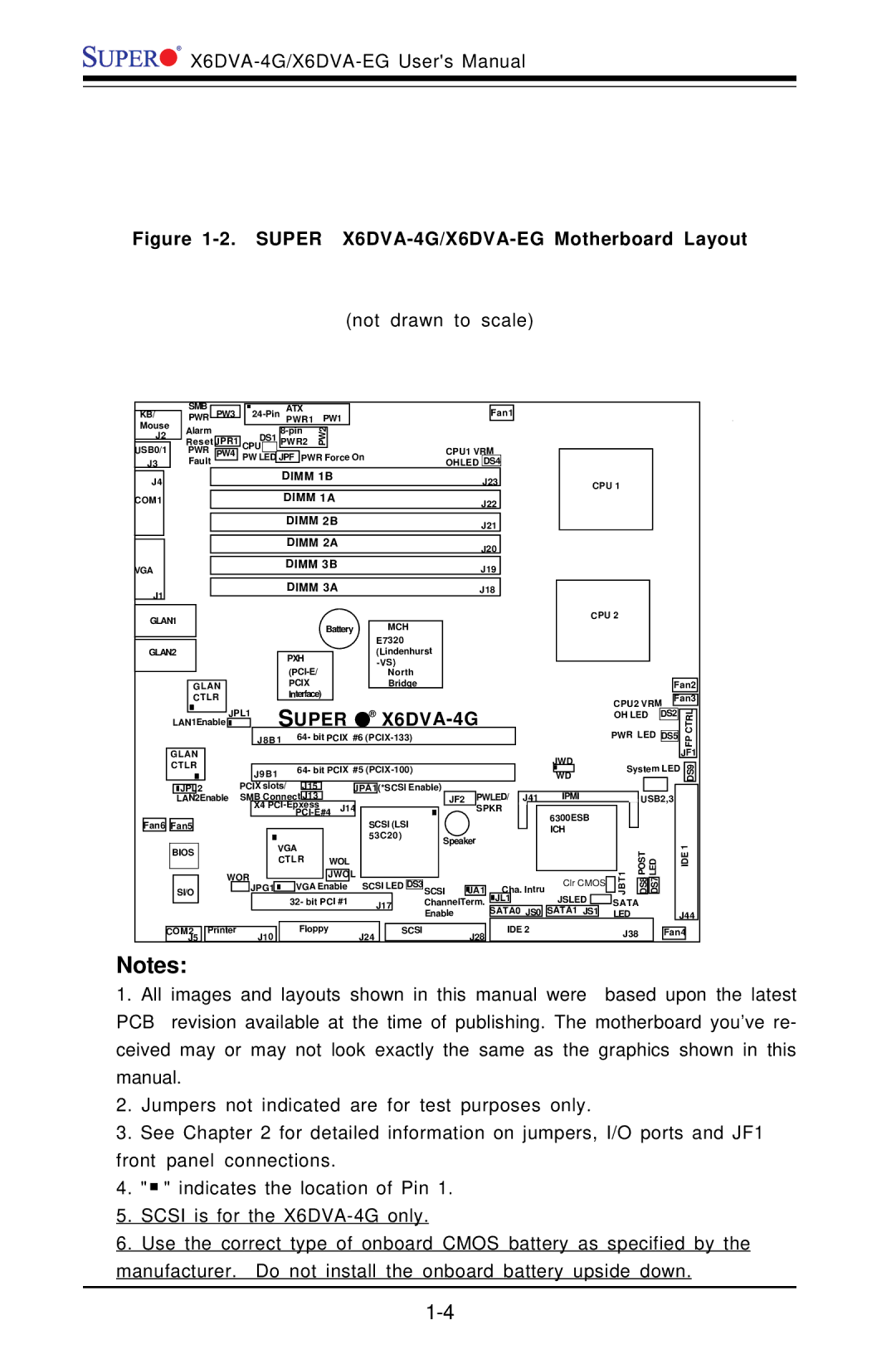
X6DVA-EG, X6DVA-4G specifications
American Megatrends is renowned for its innovative server and motherboard solutions. The X6DVA-4G and X6DVA-EG motherboards are notable examples that cater to enterprise-level applications and high-performance computing environments. Both motherboards are designed to support the latest advancements in technology while providing robust features for reliable performance.The X6DVA-4G is an ATX motherboard that boasts dual Socket 604 configurations, allowing it to support dual Intel Xeon processors. This dual-processor setup significantly enhances computing power, making it suitable for resource-intensive applications, such as virtualization, high-performance computing, and database management. Its support for up to 64GB of DDR2 ECC memory ensures data integrity and stability during critical operations, providing an additional layer of reliability that is crucial for enterprise environments.
On the other hand, the X6DVA-EG offers similar capabilities while integrating different feature sets that cater to specific needs. Both boards support PCI-X and PCIe expansion slots, which allow for flexible hardware configurations. This expandability is vital in businesses where evolving technology demands can lead to the need for additional peripherals and components.
A standout feature of these motherboards is their comprehensive support for RAID configurations, including RAID 0, 1, 10, and 5. This functionality enhances data security and recovery, ensuring that critical information remains intact in the event of hardware failure. Additionally, both motherboards come equipped with multiple SATA interfaces for robust storage options, which are essential for handling large volumes of data.
Furthermore, Intel's Xeon processors, paired with the X6DVA series motherboards, enable advanced thermal management and power efficiency features. This is essential not only for maintaining optimal performance but also for reducing operational costs in data centers.
In conclusion, American Megatrends' X6DVA-4G and X6DVA-EG motherboards maintain the company's reputation for quality and reliability in high-performance computing solutions. With their dual-processor capabilities, extensive memory support, RAID functionality, and flexibility for expansion, these motherboards are exceptional choices for businesses looking to enhance their computing infrastructure. Their combination of performance, efficiency, and reliability makes them integral components for modern server solutions.