AD620
Make vs. Buy: A Typical Bridge Application Error Budget
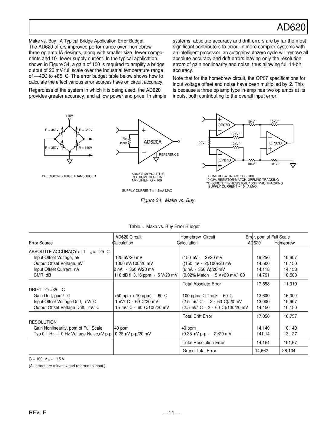
The AD620 offers improved performance over “homebrew” three op amp IA designs, along with smaller size, fewer compo- nents and 10× lower supply current. In the typical application, shown in Figure 34, a gain of 100 is required to amplify a bridge output of 20 mV full scale over the industrial temperature range of
Regardless of the system in which it is being used, the AD620 provides greater accuracy, and at low power and price. In simple
systems, absolute accuracy and drift errors are by far the most significant contributors to error. In more complex systems with an intelligent processor, an autogain/autozero cycle will remove all absolute accuracy and drift errors leaving only the resolution errors of gain nonlinearity and noise, thus allowing full
Note that for the homebrew circuit, the OP07 specifications for input voltage offset and noise have been multiplied by √2. This is because a three op amp type
| +10V |
|
|
|
|
|
|
|
| 10kV* | 10kV* |
|
|
|
| OP07D |
|
R = 350V | R = 350V |
|
|
|
|
|
|
|
| 10kV** |
|
| RG | AD620A |
|
|
|
| 499V | 100V** | 10kV** | OP07D | |
R = 350V | R = 350V |
|
|
|
|
|
| REFERENCE |
|
|
|
|
|
|
| OP07D |
|
|
|
|
| 10kV* | 10kV* |
PRECISION BRIDGE TRANSDUCER | AD620A MONOLITHIC | “HOMEBREW” |
| ||
INSTRUMENTATION |
| ||||
|
| AMPLIFIER, G = 100 | *0.02% RESISTOR MATCH, 3PPM/8C TRACKING | ||
|
|
| **DISCRETE 1% RESISTOR, 100PPM/8C TRACKING | ||
|
|
|
| SUPPLY CURRENT = 15mA MAX |
|
| SUPPLY CURRENT = 1.3mA MAX |
|
|
| |
Figure 34. Make vs. Buy
Table I. Make vs. Buy Error Budget
| AD620 Circuit | “Homebrew” Circuit | Error, ppm of Full Scale | ||
Error Source | Calculation | Calculation | AD620 |
| Homebrew |
| |||||
|
|
|
|
|
|
ABSOLUTE ACCURACY at TA = +25°C |
|
|
|
|
|
Input Offset Voltage, μV | 125 μV/20 mV | (150 μV × √2)/20 mV | 6,250 |
| 10,607 |
Output Offset Voltage, μV | 1000 μV/100/20 mV | ((150 μV × 2)/100)/20 mV | 500 |
| 150 |
Input Offset Current, nA | 2 nA × 350 Ω/20 mV | (6 nA × 350 Ω)/20 mV | 18 |
| 53 |
CMR, dB | 110 dB→3.16 ppm, × 5 V/20 mV | (0.02% Match × 5 V)/20 mV/100 | 791 |
| 500 |
|
|
|
|
|
|
|
| Total Absolute Error | 7,558 |
| 11,310 |
DRIFT TO +85°C |
|
|
|
|
|
Gain Drift, ppm/°C | (50 ppm + 10 ppm) × 60°C | 100 ppm/°C Track × 60°C | 3,600 |
| 6,000 |
Input Offset Voltage Drift, μV/°C | 1 μV/°C × 60°C/20 mV | (2.5 μV/°C × √2 × 60°C)/20 mV | 3,000 |
| 10,607 |
Output Offset Voltage Drift, μV/°C | 15 μV/°C × 60°C/100/20 mV | (2.5 μV/°C × 2 × 60°C)/100/20 mV | 450 |
| 150 |
|
|
|
|
|
|
|
| Total Drift Error | 7,050 |
| 16,757 |
RESOLUTION |
|
|
|
|
|
Gain Nonlinearity, ppm of Full Scale | 40 ppm | 40 ppm | 40 |
| 40 |
Typ 0.1 | 0.28 μV | (0.38 μV | 14 |
| 27 |
|
|
|
|
|
|
|
| Total Resolution Error | 54 |
| 67 |
|
|
|
|
|
|
|
|
|
|
|
|
|
| Grand Total Error | 14,662 |
| 28,134 |
|
|
|
|
|
|
G = 100, VS = ± 15 V. |
|
|
|
|
|
(All errors are min/max and referred to input.) |
|
|
|
|
|
REV. E |