AD620
COMMON-MODE REJECTION
Instrumentation amplifiers like the AD620 offer high CMR, which is a measure of the change in output voltage when both inputs are changed by equal amounts. These specifications are usually given for a
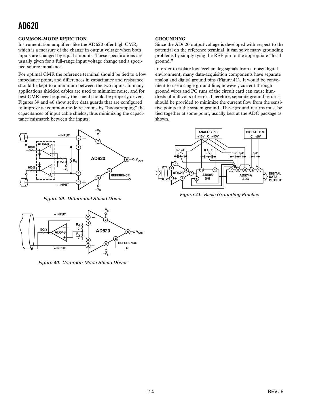
For optimal CMR the reference terminal should be tied to a low impedance point, and differences in capacitance and resistance should be kept to a minimum between the two inputs. In many applications shielded cables are used to minimize noise, and for best CMR over frequency the shield should be properly driven. Figures 39 and 40 show active data guards that are configured to improve ac
|
| +VS |
|
| – INPUT |
|
|
100V | AD648 |
|
|
|
|
| |
| RG | AD620 | VOUT |
100V |
|
| |
| S |
|
|
|
|
| REFERENCE |
+ INPUT
S
Figure 39. Differential Shield Driver
GROUNDING
Since the AD620 output voltage is developed with respect to the potential on the reference terminal, it can solve many grounding problems by simply tying the REF pin to the appropriate “local ground.”
In order to isolate low level analog signals from a noisy digital environment, many
ANALOG P.S. |
| DIGITAL P.S. |
+15V C |
| C +5V |
0.1mF | 0.1mF |
|
|
| 1mF | 1mF | 1mF |
|
|
| + |
AD620 | AD585 | AD574A | DIGITAL |
| DATA | ||
| S/H | ADC | |
| OUTPUT | ||
|
|
|
Figure 41. Basic Grounding Practice
| – INPUT |
|
|
| RG |
100V | AD548 | 2 |
| ||
| RG | |
|
| |
|
| 2 |
| + INPUT |
|
+VS
AD620 | VOUT |
| REFERENCE |
| |
S |
|
Figure 40. Common-Mode Shield Driver
REV. E |