AD620 |
. . . . . . . . . . . . . . . . . . . . . . . . . . . . . . . . . . . . . . . . |
. . . . . . . . . . . . . . . . . . . . . . . . . . . . . . . . . . . . . . . . |
Figure 31b. Gain Nonlinearity, G = 100, RL = 10 kΩ |
(100 μV = 10 ppm) |
. . . . . . . . . . . . . . . . . . . . . . . . . . . . . . . . . . . . . . . . |
. . . . . . . . . . . . . . . . . . . . . . . . . . . . . . . . . . . . . . . . |
Figure 31c. Gain Nonlinearity, G = 1000, RL = 10 kΩ | |||||
(1 mV = 100 ppm) |
|
|
| ||
|
|
| 10kV* | 1kV | 10kV |
INPUT |
|
| 10T | ||
|
|
|
|
| |
10V |
|
|
|
|
|
100kV |
|
|
|
| VOUT |
|
|
|
|
| |
|
|
|
| +VS |
|
11kV | 1kV | 100V | 2 |
|
|
|
|
| |||
|
|
| 1 | 7 |
|
| G=1000 | G=1 |
|
| |
|
| G=100 | G=10 | AD620 | 6 |
|
|
|
|
| |
| 49.9V 499V | 5.49kV |
| 5 | |
|
|
| 8 |
| |
|
|
| 4 |
| |
|
|
| 3 |
| |
|
|
|
|
| |
I1 | 20mA | VB | 20mA | I2 |
|
|
| A1 |
| A2 |
| 10kV |
|
|
|
|
|
|
| |
| C1 |
| C2 |
|
|
|
|
|
|
| 10kV |
|
|
|
|
|
|
| A3 | OUTPUT |
R3 | R1 | R2 | 10kV | 10kV | REF | |
|
| |||||
400V |
|
| ||||
|
|
|
|
|
| |
– IN | Q1 |
|
| Q2 | +IN |
|
|
| RG |
| R4 |
|
|
|
|
| 400V |
|
| |
| GAIN |
| GAIN |
|
|
|
| SENSE |
| SENSE |
|
|
|
|
|
|
|
| ||
|
| S |
|
|
| |
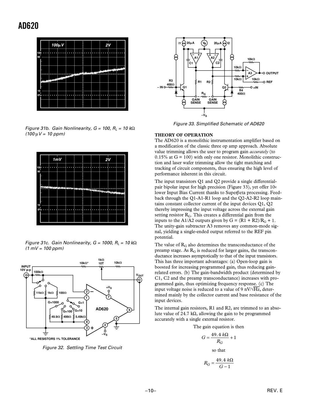
Figure 33. Simplified Schematic of AD620
THEORY OF OPERATION
The AD620 is a monolithic instrumentation amplifier based on a modification of the classic three op amp approach. Absolute value trimming allows the user to program gain accurately (to 0.15% at G = 100) with only one resistor. Monolithic construc- tion and laser wafer trimming allow the tight matching and tracking of circuit components, thus ensuring the high level of performance inherent in this circuit.
The input transistors Q1 and Q2 provide a single differential- pair bipolar input for high precision (Figure 33), yet offer 10× lower Input Bias Current thanks to Superβeta processing. Feed- back through the
The value of RG also determines the transconductance of the preamp stage. As RG is reduced for larger gains, the transcon- ductance increases asymptotically to that of the input transistors. This has three important advantages: (a)
The internal gain resistors, R1 and R2, are trimmed to an abso- lute value of 24.7 kΩ, allowing the gain to be programmed accurately with a single external resistor.
The gain equation is then
S |
*ALL RESISTORS 1% TOLERANCE |
Figure 32. Settling Time Test Circuit
= 8>28 Ω +
so that
5
=8>28 Ω
−5
REV. E |