1

2

3

4

5

6

7

8


+5V_D

D


+5V_D


14


TH100


+ C102

PTH90DEG


IC100G

C100

C101

IC100E

74HC14D

100N SM

100U EL

100N SM


11

10

THERMPROT

7

R100

74HC14D


1K0 SM


IC100F


13

12

SK100

TP102


1

TP103


2


3


4


0V_D

5

SPKR1 ON

TP104

6

SPKR2 ON


TP105


7

THERMPROT


TP106


8

VIPROT1


TP107


9

DCPROT1


TP108


10


11

+5V_D


12


13


14


0V_SIG

R107


0V_D


FFC 14W 2.54MM VER


SP100

2R2 SM

PIN 1 TO THE LEFT AS YOU LOOK FROM THE FRONT

TP116

0V_D


0V_LS

STAR POINT 8 0V_HF


0V_PSU


D

C

B

A

0V_D74HC14D


IC100A

IC100B


+49V


R101


1


23


4


VIPROT1


1K0 SM


C103


74HC14D

74HC14D


10N SM


D100

RLY101B


RLY100B


IC100C

IC100D


RLY SPST SPKR


RLY SPST SPKR

D101


R102


1N4003F


5


69


8


DCPROT1


1N4003F


1K0 SM


C104


74HC14D

74HC14D


10N SM


SK101

TP109


1

L911C2_1


TR100

TR101


R105

SPKR1 ON


F


L911C2_1.1.SCH


INPUT

VIPROT


BD179

BD179


100R SM


0V_D


0V_SIG

DCPROT

TP111


EMC


SK102A


TP113 SK102B


N

+49V

0V_LS

OUTPUT


RLY101A

TP112


RLY100A


C105

0V_HF


Top+


Bot+


R106


VPOS


SPKR2 ON


1N0 SM


100R SM


PHONO2G


VNEG


RLY SPST SPKR


RLY SPST SPKR


-49V


R103


R104


0V_SIG

TP110


0V_HF


Top-


Bot-


220R SM


220R SM


0V_LS


0V_LS


0V_D


+49V


TP100


1

BR100


TP114


BRGBU8D

+ C106


PB


+


C108


10,000u 63V


100N PC


PCB


1

2


3

~


~

2


L911PB_1


+ C107


0V_PSU


SK103


-


10,000u 63V


C109


MOLEXPWR4


4


TP101


3

4


100N PC


DRAWING TITLE


TP115


POWER AMP SUPPLY


AP85 third channel - top level


23425


Circuit Diagram


-49V


Notes:


01_1101


JR

4/6/01


DC OFFSET CHANGES


1.1


A & R Cambridge Ltd.


Pembroke Avenue


01_1018


JR

30/1/01

PRODUCTION ISSUE


1.0


Denny Industrial Centre


ECO No.

INITIALS

DATE


DESCRIPTION OF CHANGE

ISSUE


Waterbeach


Filename


Date Printed


Drawn by:


Cambridge CB5 9PB


Sheet 1 of 2

DRAWING NO. L911C1


J:\ECO_wip\01_1101 A85 RANGE PCB FUSES AND DC OFFSET\L911_1.1.DDB - Documents\L911C14-Jun-2001.1.PRJ

J Reckless


1


2


3


4


5


6


7


8


C

B

A

Page 23
Image 23
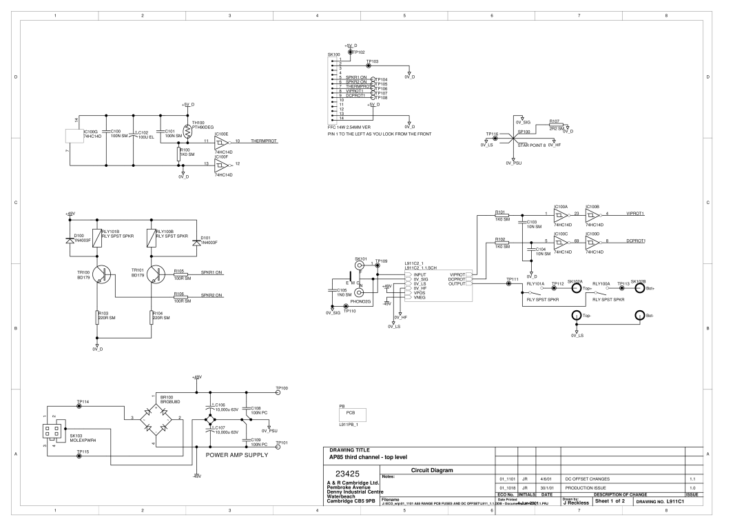
Arcam A85 service manual AP85 third channel top level

A85 specifications

The Arcam P85 and A85 amplifiers are a testament to Arcam's commitment to high-quality audio performance. These components are well-known in the audiophile community for their unique blend of state-of-the-art technology and superior sound quality, catering to discerning listeners who value fidelity and craftsmanship.

The Arcam A85 is a high-performance integrated amplifier that features a robust design and advanced circuitry. It offers a powerful 85 watts per channel output, which is more than sufficient to drive a wide range of speakers with clarity and precision. The A85 incorporates a dual mono design with separate power supplies for the left and right channels, ensuring low crosstalk and high channel separation. This design choice also enhances the amplifier’s dynamic response, allowing it to handle complex musical passages with ease.

One of the standout features of the A85 is its use of high-quality components, including low-noise transistors and capacitors that are specifically chosen to minimize distortion. The amplifier exhibits an impressive signal-to-noise ratio, contributing to a clean audio signal that preserves the nuances of the music.

On the other hand, the Arcam P85 is a powerful, dedicated power amplifier that pairs perfectly with the A85. It utilizes a Class G amplification technology, which provides significant power efficiency. This means that the P85 can deliver peak power output without generating excessive heat, making it an ideal choice for long listening sessions.

The P85 offers 85 watts per channel into 8 ohms but can also deliver 140 watts into 4 ohms, allowing it to drive even the most demanding loudspeakers with authority. Its balanced XLR inputs, alongside standard RCA inputs, ensure compatibility with various audio sources, while the sturdy construction ensures durability and performance.

Both the A85 and P85 feature a simple yet elegant design, characterized by a sleek chassis that minimizes resonances and maximizes aesthetic appeal. They also come equipped with a variety of connection options, including multiple line-level inputs and outputs, making integration into an existing audio system straightforward.

In summary, the Arcam P85 and A85 amplifiers represent a harmonious fusion of innovative technology, impeccable sound quality, and user-friendly design. Their powerful performance, combined with high efficiency and low distortion, makes them a prized possession for any audiophile seeking to enhance their listening experience. Whether used in a stereo setup or as part of a more extensive home theater system, the A85 and P85 deliver exceptional audio performance that stands the test of time.