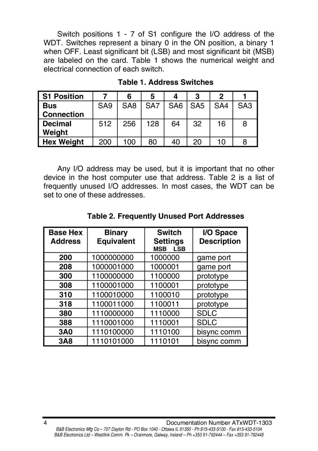
Switch positions 1 - 7 of S1 configure the I/O address of the WDT. Switches represent a binary 0 in the ON position, a binary 1 when OFF. Least significant bit (LSB) and most significant bit (MSB) are labeled on the card. Table 1 shows the numerical weight and electrical connection of each switch.
Table 1. Address Switches
S1 Position | 7 | 6 | 5 | 4 | 3 | 2 | 1 |
Bus | SA9 | SA8 | SA7 | SA6 | SA5 | SA4 | SA3 |
Connection |
|
|
|
|
|
|
|
Decimal | 512 | 256 | 128 | 64 | 32 | 16 | 8 |
Weight |
|
|
|
|
|
|
|
Hex Weight | 200 | 100 | 80 | 40 | 20 | 10 | 8 |
Any I/O address may be used, but it is important that no other device in the host computer use that address. Table 2 is a list of frequently unused I/O addresses. In most cases, the WDT can be set to one of these addresses.
Table 2. Frequently Unused Port Addresses
Base Hex | Binary | Switch | I/O Space |
Address | Equivalent | Settings | Description |
|
| MSB LSB |
|
200 | 1000000000 | 1000000 | game port |
208 | 1000001000 | 1000001 | game port |
300 | 1100000000 | 1100000 | prototype |
308 | 1100001000 | 1100001 | prototype |
310 | 1100010000 | 1100010 | prototype |
318 | 1100011000 | 1100011 | prototype |
380 | 1110000000 | 1110000 | SDLC |
388 | 1110001000 | 1110001 | SDLC |
3A0 | 1110100000 | 1110100 | bisync comm |
3A8 | 1110101000 | 1110101 | bisync comm |
4 | Documentation Number |
B&B Electronics Mfg Co – 707 Dayton Rd - PO Box 1040 - Ottawa IL 61350 - Ph