CY62148BN MoBL®
Maximum Ratings
(Above which the useful life may be impaired. For user guide- lines, not tested.)
Storage Temperature | ||
Ambient Temperature with |
|
|
Power Applied | ||
Supply Voltage on VCC to Relative GND | ||
DC Voltage Applied to Outputs |
|
|
in High Z State[2] | +0.5V | |
DC Input Voltage[2] | CC |
|
+0.5V | ||
| CC |
|
Electrical Characteristics Over the Operating Range
Current into Outputs (LOW) | 20 mA |
Static Discharge Voltage | 2001V |
(per |
|
>200 mA |
Operating Range
| Ambient [3] | VCC |
Range | Temperature | |
Commercial | 0°C to +70°C | |
|
|
|
Industrial |
| |
|
|
|
|
|
|
|
|
|
|
|
|
| |||
Parameter | Description | Test Conditions |
|
|
|
|
|
| Unit | |||
| Min. |
| Typ.[1] |
| Max. | |||||||
VOH | Output HIGH Voltage | VCC = Min., IOH = – 1 mA |
| 2.4 |
|
|
|
| V | |||
VOL | Output LOW Voltage | VCC = Min., IOL = 2.1 mA |
|
|
|
|
| 0.4 | V | |||
VIH | Input HIGH Voltage |
|
|
|
|
| 2.2 |
|
|
| VCC+0.3 | V |
VIL | Input LOW Voltage |
|
|
|
|
|
|
|
| 0.8 | V | |
IIX | Input Leakage Current | GND ≤ VI ≤ VCC |
|
|
|
|
| +1 | ∝A | |||
IOZ | Output Leakage Current | GND ≤ VI ≤ VCC, Output Disabled |
|
|
| +1 | ∝A | |||||
ICC | VCC Operating | f = fMAX = 1/tRC | Com’l/Ind’l |
|
| 12.5 |
| 20 | mA | |||
| Supply Current |
|
|
| IOUT | =0 mA |
|
|
|
|
|
|
| f = 1 MHz |
|
|
|
| 2.5 |
|
| mA | |||
|
|
|
|
| VCC | = Max., |
|
|
|
|
|
|
ISB1 | Automatic CE | Max. VCC |
| ≤ VIH | Com’l/ |
|
|
|
| 1.5 | mA | |
,CE |
|
|
|
| ||||||||
| VIN ≤ VIH or VIN ≤ VIL, | Ind’l |
|
|
|
|
|
|
| |||
| f = fMAX |
|
|
|
|
|
|
|
|
|
| |
ISB2 | Automatic CE | Max. VCC, | – 0.3V, | Com’l/ |
|
| 4 |
| 20 | ∝A | ||
| CE ≤ VCC | Ind’l |
|
|
|
|
|
|
| |||
| VIN ≤ VCC | – 0.3V, |
|
|
|
|
|
|
|
| ||
|
| or VIN ≤ 0.3V, f =0 |
|
|
|
|
|
|
|
| ||
Capacitance[4]
Parameter | Description | Test Conditions | Max. | Unit |
CIN | Input Capacitance | TA = 25°C, f = 1 MHz, | 6 | pF |
|
| VCC = 5.0V |
|
|
COUT | Output Capacitance | 8 | pF |
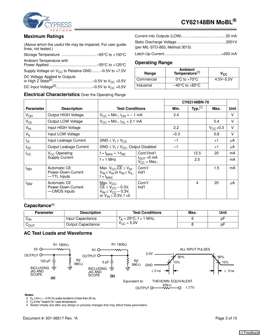
AC Test Loads and Waveforms
R1 1800Ω
5V |
OUTPUT |
100 pF ![]()
INCLUDING
JIG AND
SCOPE
(a)
|
| R1 1800Ω |
| |
5V |
|
| ALL INPUT PULSES | |
OUTPUT |
|
| 3.0V | |
|
| 90% | ||
R2 | 5 pF | R2 | 10% | |
990 Ω | 990 Ω | |||
| GND |
INCLUDING |
|
|
|
|
|
|
|
|
|
|
|
| ≤ 3 ns |
|
|
|
|
|
| ||
|
|
|
|
|
|
|
|
|
|
|
|
|
|
|
|
|
| ||||
|
|
|
|
|
|
|
|
|
|
|
|
|
|
|
|
|
| ||||
JIG AND |
| (b) |
|
|
|
|
|
| |||||||||||||
|
|
|
|
|
| ||||||||||||||||
SCOPE |
|
|
|
|
|
|
|
|
|
| |||||||||||
|
|
|
|
|
| Equivalent to: | THEVENIN EQUIVALENT | ||||||||||||||
|
|
|
|
|
|
|
|
|
|
|
| OUTPUT |
| 639 Ω |
|
| 1.77V | ||||
|
|
|
|
|
|
|
|
|
|
|
|
|
|
|
|
|
|
|
| ||
90%
10%
≤ 3 ns
Notes:
2.VIL (min.) =
3.TA is the “Instant On” case temperature
4.Tested initially and after any design or process changes that may affect these parameters.
Document #: | Page 3 of 10 |
[+] Feedback