CY62148BN MoBL®
Data Retention Characteristics (Over the Operating Range)
Parameter | Description |
|
| Conditions | Min. | Typ.[1] | Max. | Unit | |
VDR | VCC for Data Retention |
|
|
| 2.0 |
|
| V | |
ICCDR | Data Retention Current |
| Com’l | LL | No input may exceed |
|
| 20 | ∝A |
|
|
|
|
| VCC + 0.3V |
|
|
|
|
|
|
| Ind’l | LL |
|
| 20 | ∝A | |
|
|
|
|
| VCC = VDR = 3.0V |
|
|
|
|
tCDR[4] |
|
|
|
|
|
|
|
| |
Chip Deselect to Data Retention Time | CE > VCC – 0.3V | 0 |
|
| ns | ||||
|
|
|
| VIN > VCC – 0.3V or |
|
|
|
| |
tR[9] | Operation Recovery Time |
|
| tRC |
|
| ns | ||
|
|
|
|
| VIN < 0.3V |
|
|
|
|
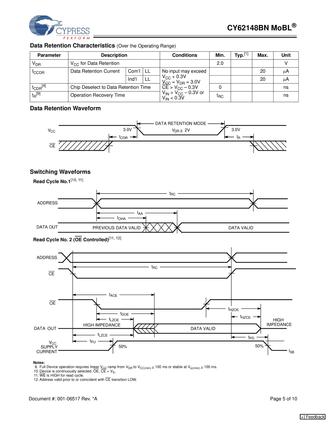
Data Retention Waveform
![]() DATA RETENTION MODE
DATA RETENTION MODE ![]()
VCC | 3.0V | VDR > 2V | 3.0V |
| tCDR |
| tR |
CE |
|
|
|
Switching Waveforms
Read Cycle No.1[10, 11]
ADDRESS |
|
|
|
|
|
|
|
|
|
|
|
|
| tRC |
|
|
|
|
|
|
| ||||
|
|
|
|
|
|
|
|
|
|
|
|
|
|
|
|
|
|
|
| ||||||
|
|
|
|
|
|
|
|
|
|
|
|
|
|
|
|
|
|
|
|
|
|
|
|
| |
|
|
|
|
|
|
|
|
|
|
|
|
|
|
|
|
|
|
|
|
|
|
|
|
| |
|
|
|
|
|
|
|
|
|
|
|
|
|
|
|
|
|
|
|
|
|
|
|
|
| |
|
|
|
|
|
|
|
|
|
|
|
|
|
|
|
|
|
|
|
|
|
|
|
|
|
|
|
|
|
|
|
|
|
|
|
|
|
|
|
|
|
|
|
|
|
|
|
|
|
|
| |
|
|
|
|
|
|
|
|
| tAA |
|
|
|
|
|
|
|
|
|
|
|
|
|
|
| |
DATA OUT |
|
|
|
|
|
| tOHA |
|
|
|
|
|
|
|
|
|
|
|
|
|
|
|
| ||
|
|
|
|
|
|
|
|
|
|
|
|
|
|
|
|
|
|
|
|
| |||||
PREVIOUS DATA VALID |
|
|
|
|
|
|
|
|
| DATA VALID | |||||||||||||||
|
|
|
|
|
|
|
|
| |||||||||||||||||
|
|
|
|
|
|
|
|
|
|
|
|
|
|
|
|
|
|
|
|
|
|
|
|
|
|
|
|
|
|
|
|
|
|
|
|
|
|
|
|
|
|
|
|
|
|
|
|
|
|
|
|
Read Cycle No. 2 (OE Controlled)[11, 12]
ADDRESS |
|
|
|
|
| tRC |
|
CE |
|
|
|
| tACE |
|
|
OE |
| tHZOE |
|
| tDOE |
| |
| tHZCE |
| |
| tLZOE | HIGH | |
DATA OUT | HIGH IMPEDANCE | DATA VALID | IMPEDANCE |
|
| ||
| tLZCE | tPD |
|
VCC | tPU |
| |
| 50% | ||
SUPPLY | 50% |
| |
CURRENT |
|
| ISB |
Notes:
9. Full Device operation requires linear VCC ramp from VDR to VCC(min) > 100 ms or stable at Vcc(min) > 100 ms. 10. Device is continuously selected. OE, CE = VIL.
11. WE is HIGH for read cycle.
12. Address valid prior to or coincident with CE transition LOW.
Document #: | Page 5 of 10 |
[+] Feedback