CY62157ESL MoBL®
Data Retention Characteristics
Over the Operating Range
| Parameter | Description |
|
| Conditions |
| Min | Typ[2] | Max | Unit |
VDR | VCC for Data Retention |
|
|
|
| 1.5 |
|
| V | |
ICCDR | Data Retention Current |
|
| > VCC – 0.2V, | VCC = 1.5V |
| 2 | 5 | μA | |
| CE |
| ||||||||
|
|
|
| VIN > VCC – 0.2V or VIN < 0.2V |
|
|
|
|
| |
|
|
|
| VCC = 2.0V |
| 2 | 8 |
| ||
|
|
|
|
|
|
|
| |||
tCDR [6] | Chip Deselect to Data |
|
|
|
| 0 |
|
| ns | |
|
| Retention Time |
|
|
|
|
|
|
|
|
|
|
|
|
|
|
|
|
|
|
|
t | [7] | Operation Recovery Time |
|
|
|
| t |
|
| ns |
| R |
|
|
|
|
| RC |
|
|
|
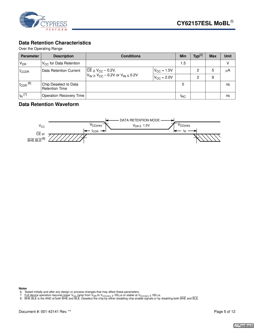
Data Retention Waveform
|
| VCC(min) | DATA RETENTION MODE | VCC(min) | |
V | CC | V | > 1.5V | ||
| tCDR | DR |
| tR | |
CE or |
|
| |||
|
|
|
| ||
BHE.BLE [8] |
|
|
|
| |
Notes
6.Tested initially and after any design or process changes that may affect these parameters.
7.Full device operation requires linear VCC ramp from VDR to VCC(min) > 100 μs or stable at VCC(min) > 100 μs.
8.BHE.BLE is the AND of both BHE and BLE. Deselect the chip by either disabling chip enable signals or by disabling both BHE and BLE.
Document #: | Page 5 of 12 |
[+] Feedback